Test circuit for display device

A technology for testing circuits and display devices, applied to static indicators, instruments, etc., can solve the problems of multiple power supply signal pads, shunt switches hanging in the air, etc., to achieve the effects of ensuring accuracy, reducing quantity, and reducing difficulty

Active Publication Date: 2013-08-28
XIAMEN TIANMA MICRO ELECTRONICS
View PDF7 Cites 10 Cited by
  • Summary
  • Abstract
  • Description
  • Claims
  • Application Information

AI Technical Summary

Problems solved by technology

[0003] The purpose of the present invention is to provide a test circuit for display device pixel array, to solve the test ci

Method used


Image

  • Test circuit for display device
  • Test circuit for display device
  • Test circuit for display device

Examples


Embodiment Construction

[0018] The implementation process of the embodiment of the present invention will be described in detail below in conjunction with the accompanying drawings.

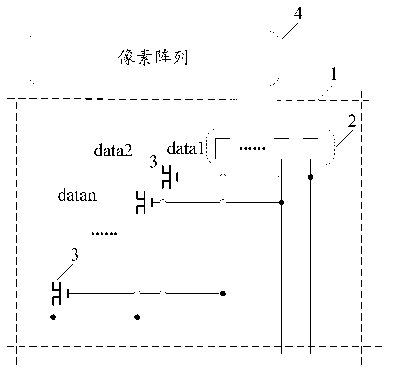
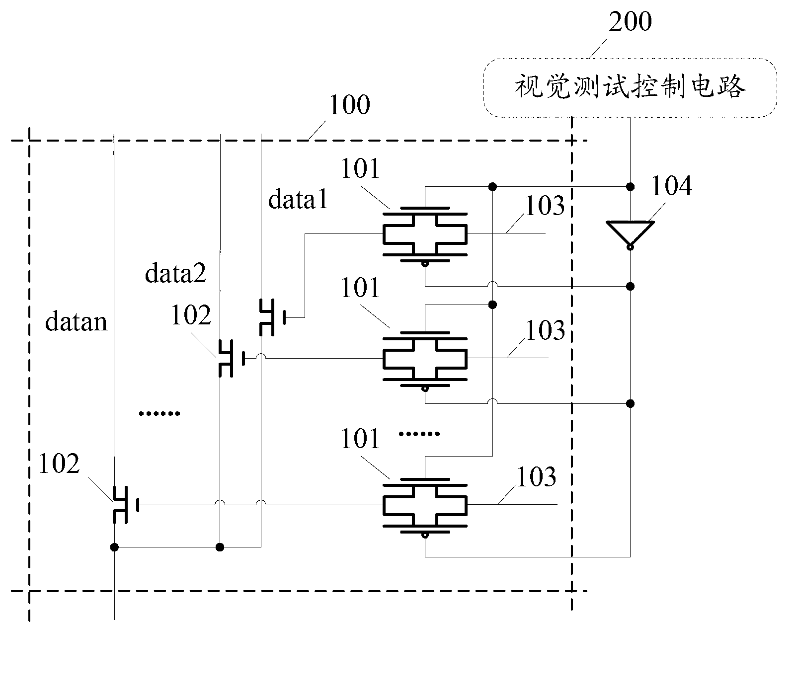
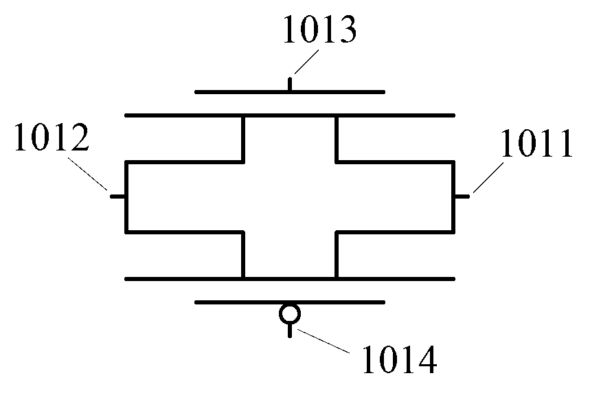
[0019] Embodiment 1 of the present invention provides a test circuit for a display device, such as Figure 2A As shown, it includes a plurality of array test circuits 100 and a visual test control circuit 200. The array test circuit 100 includes a plurality of CMOS transmission gates 101 and a plurality of shunt switches 102; where reference Figure 2B The enlarged schematic diagram of the CMOS transmission gate 101 is shown. The CMOS transmission gate 101 includes an input terminal 1011 , an output terminal 1012 , a first control terminal 1013 and a second control terminal 1014 .

[0020] The input terminal 1011 of the CMOS transmission gate 101 is connected to the power signal 103, the output terminal 1012 is connected to the shunt switch 102, the first control terminal 1013 and the second control terminal 1014 are re...


PUM


Abstract

The invention discloses a test circuit for a display device, comprising multiple array test circuits and a vision test control circuit, wherein each array test circuit comprises multiple CMOS (complementary metal oxide semiconductor) transmission gates and multiple branch switches; the input end of each CMOS transmission gate is connected with a power signal, the output end of each CMOS transmission gate is connected with the corresponding branch switch, and a first control end and a second control end are respectively connected with an output signal of the vision test control circuit and the inverted signal of the output signal of the vision test control circuit; and the vision test control circuit is used for controlling the branch switches to switch off through the CMOS transmission gates during vision test. When the test circuit is used for carrying out a vision test, the branch switches of array test circuits are not suspended in midair, so that the test circuit is not interfered by the outside environment, and the accuracy of the test result is guaranteed; and meanwhile, the number of power signal gaskets is reduced, and the difficulty in selecting IC (integrated circuit) or FPC (flexible printed circuit) during design is reduced.

Description

technical field [0001] The invention relates to the field of display device testing, in particular to a test circuit of a display device. Background technique [0002] In the test circuit of the liquid crystal display, the visual test and the pixel array test respectively adopt independent switching signals, and when the visual test is performed, the shunt switch for controlling the pixel array test and the array test is in a suspended state. Such as figure 1 As shown, the test circuit includes an array test circuit 1, which is connected to a pixel array 4, wherein the array test circuit 1 includes a plurality of integrated circuit elements IC (Integrate Circuit) or flexible circuit board FPC pads 2, and a plurality of corresponding A shunt switch 3; the IC or FPC pad 2 is connected to the shunt switch 3 in one-to-one correspondence, and is used to control the opening or closing of the shunt switch through the input power signal. Since the test circuit is in the visual tes...

Claims


Application Information

Patent Timeline
IPC IPC(8): G09G3/00
Inventor 夏军吴昊
Owner XIAMEN TIANMA MICRO ELECTRONICS
Why Eureka
Try Eureka