Field-effect transistor, edge structure and related manufacturing method

A technology of field effect transistors and transistor units, applied in semiconductor/solid-state device manufacturing, semiconductor devices, electrical components, etc., can solve the problems of reduced reliability and durability, reverse breakdown voltage drift of field effect transistors 10, failure to achieve design Requirements and other issues to achieve the effect of improving the service life and solving the problem of easy breakdown

Active Publication Date: 2016-04-06
CHENGDU MONOLITHIC POWER SYST
View PDF4 Cites 0 Cited by
  • Summary
  • Abstract
  • Description
  • Claims
  • Application Information

AI Technical Summary

Problems solved by technology

Therefore, the existence of the strong electric field region on the left side of the leftmost trench type isolation unit 109 will cause the reverse breakdown voltage of the field effect transistor 10 to drift or decrease, which cannot meet the expected design requirements.
In addition, during use, the leftmost trench isolation unit 109 of the field effect transistor 10 may repeatedly withstand a strong voltage for a long time, so the reliability and durability will also be reduced, affecting the service life of the field effect transistor 10

Method used


Image

  • Field-effect transistor, edge structure and related manufacturing method
  • Field-effect transistor, edge structure and related manufacturing method
  • Field-effect transistor, edge structure and related manufacturing method

Examples


Embodiment Construction

[0026] Some embodiments of the present disclosure will be described in detail below with reference to the accompanying drawings. It should be understood, however, that these descriptions are exemplary only, and are not intended to limit the scope of the present disclosure. Also, descriptions of well-known structures and techniques are omitted in the following description to avoid unnecessarily obscuring the concepts of the present disclosure.

[0027] In the following description, some specific details, such as the specific circuit structure, device structure, process steps and specific parameters of these circuits, devices and processes in the embodiments, are used to provide a better understanding of the embodiments of the present disclosure . It will be understood by those skilled in the art that the embodiments of the present disclosure may be practiced even without some details or in combination with other methods, elements, materials, and the like.

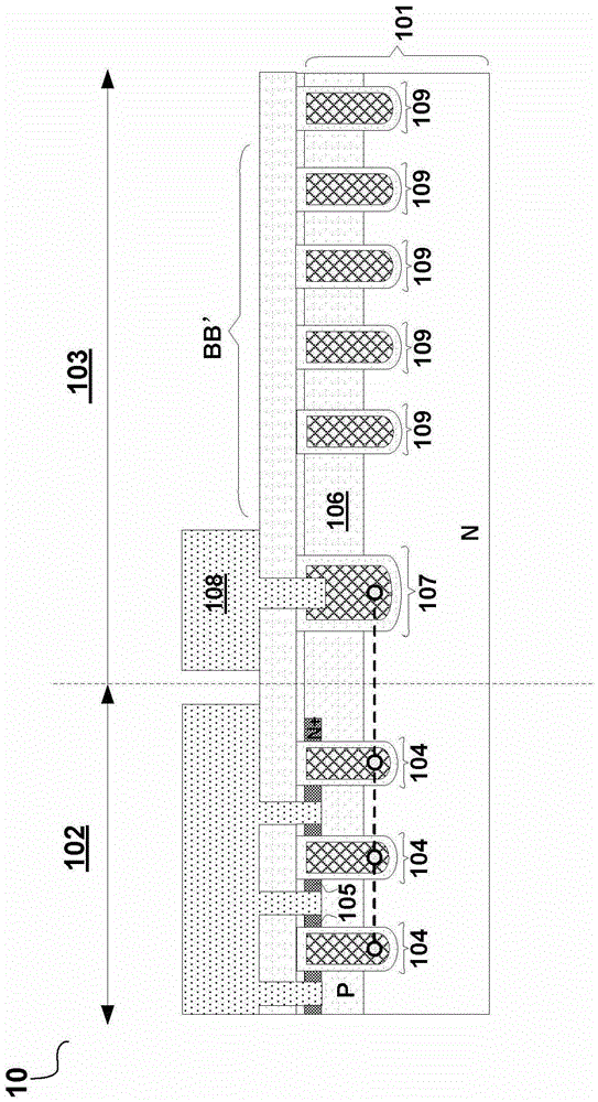
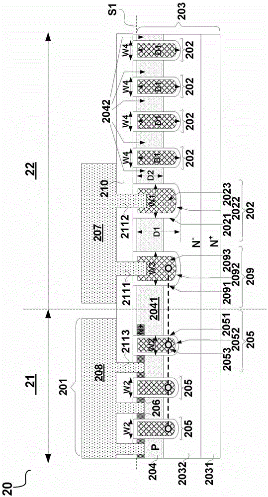
[0028] In the desc...


PUM


Abstract

A field effect transistor (“FET”), a termination structure and associated method for manufacturing. The FET has a plurality of active transistor cells and a termination structure. The termination structure for the FET includes a plurality of termination cells arranged substantially in parallel from an inner side toward an outer side of a termination area of the FET. Each of the termination cells comprises a termination trench lined with a termination insulation layer and filled with a termination conduction layer. The innermost termination cell is electrically coupled to gate regions of the active transistor cells while the rest of the termination cells are electrically floating.

Description

technical field [0001] Embodiments of the present disclosure relate to semiconductor devices, particularly but not limited to field effect transistors and methods of manufacturing the same. Background technique [0002] Semiconductor devices such as Metal Oxide Semiconductor Field Effect Transistor (MOSFET), Junction Field Effect Transistor (JFET) and Double Diffused Metal Oxide Semiconductor Field Effect Transistor (DMOS) have been widely used in the electronics industry. In some applications, such as power switches for switching voltage converters, field effect transistors should have good current handling capabilities, low on-resistance Rds ON , higher breakdown voltage BV and good safety and durability. [0003] Field effect transistors such as MOSFETs, JFETs, DMOSs, etc. are usually fabricated on a semiconductor substrate and have an active cell area and an edge area. The effective cell area includes at least one field effect transistor unit, has a gate area, a source...

Claims


Application Information

Patent Timeline
Patent Type & Authority Patents(China)
IPC IPC(8): H01L29/06H01L29/772H01L29/78H01L21/335
CPCH01L29/0634H01L29/0619H01L29/407H01L29/41766H01L29/4236H01L29/4238H01L29/66727H01L29/66734H01L29/7811H01L29/7813
Inventor 马荣耀李铁生王怀锋
Owner CHENGDU MONOLITHIC POWER SYST
Why Eureka
Try Eureka