Super-thin broadband wave-absorbing metamaterial

A metamaterial and broadband technology, applied in the direction of electrical components, magnetic field/electric field shielding, etc., can solve problems such as unfavorable actual production and manufacturing, small structure, and unsuitability

Inactive Publication Date: 2013-08-28
UNIV OF ELECTRONICS SCI & TECH OF CHINA
View PDF4 Cites 22 Cited by
  • Summary
  • Abstract
  • Description
  • Claims
  • Application Information

AI Technical Summary

Problems solved by technology

Although the method of increasing the lumped capacitance and resistance is a novel and applicable method, the use of this method is not conducive to the actual production
For terahertz, infrared, and light wave frequency bands, the structure of absorbing metamaterials is getting smaller and smaller, and this method of adding lumped elements to expand bandwidth is even more inappropriate.

Method used


Image

  • Super-thin broadband wave-absorbing metamaterial
  • Super-thin broadband wave-absorbing metamaterial
  • Super-thin broadband wave-absorbing metamaterial

Examples


Embodiment Construction

[0014] An ultra-thin broadband wave-absorbing metamaterial according to a specific embodiment of the present invention will be further described below in conjunction with the accompanying drawings.

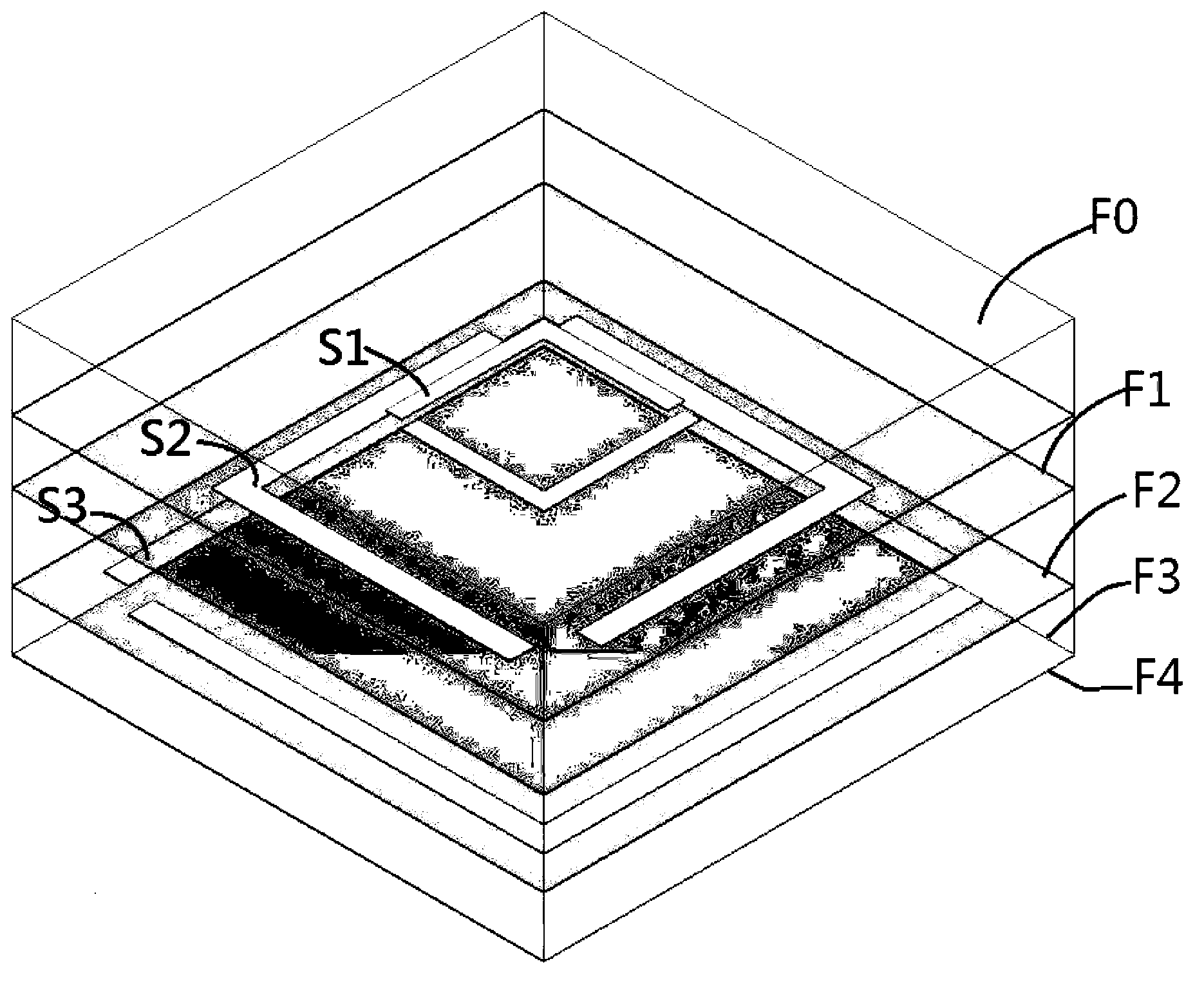
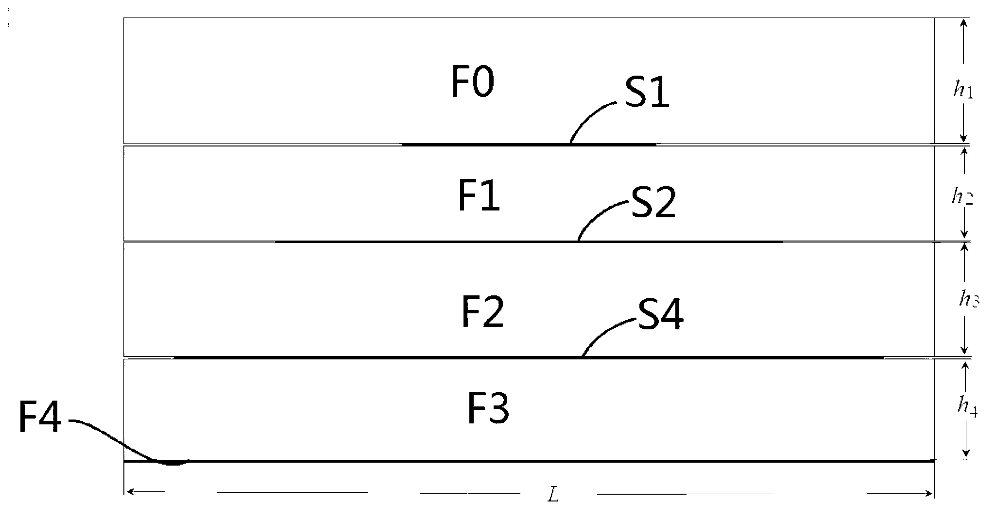
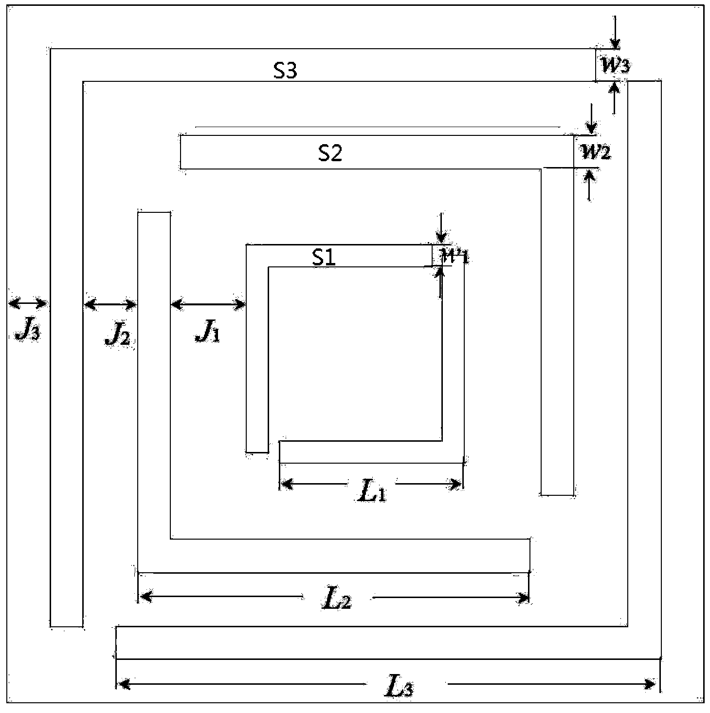
[0015] like figure 1 , figure 2 and image 3 As shown, an ultra-thin broadband absorbing metamaterial in this embodiment includes at least two layers of dielectric plates stacked together, labeled F1, F2 and F3 in the figure, and among the stacked dielectric plates, the top layer The upper surface of the dielectric board F1 is covered with a layer of matching layer F0, the lower surface of the dielectric board F3 at the bottom is covered with a layer of metal floor F4, and the upper surface of each layer of dielectric board also includes a layer of non-closed ring metal layer, the label in the figure are S1, S2 and S3, the non-closed annular metal layers (S1, S2 and S3) on different dielectric plates have the same shape and different sizes, and are arranged in a pyramid structu...


PUM


Abstract

The invention discloses super-thin broadband wave-absorbing metamaterial. The super-thin broadband wave-absorbing metamaterial comprises at least two layers of dielectric slabs which are laminated together. In the laminated dielectric slabs, a matching layer covers the upper surface of the dielectric slab at the top layer, a metal floor layer covers the lower surface of the dielectric slab at the bottom layer, and a non-closed annular metal layer further covers the upper surface of the dielectric slab at each layer. The non-closed annular metal layers located on the different dielectric slabs are same in shapes and mutually different in terms of sizes. The non-closed annular metal layers are distributed according to the pyramid structure, wherein the non-closed annular metal layer with the largest size is located on the dielectric slab at the bottom layer. According to the wave-absorbing metamaterial, due to the fact that electromagnetic parameters of each layer of structure are changed, phase positions of a reflected wave and a refracted wave are changed. Therefore, a final reflected wave and an incident wave are counteracted, so that the same effect that electromagnetic waves are absorbed by the metamaterial is achieved. Due to the fact that a metamaterial structure composed of the three dielectric slabs, three metal rings and the metal floor is adopted, the broadband wave-absorbing metamaterial is super-thin.

Description

technical field [0001] The invention relates to the technical field of metamaterial microwave absorption, in particular to an ultra-thin broadband microwave-absorbing metamaterial. Background technique [0002] Absorbing material refers to a class of materials that can absorb most of the energy of electromagnetic waves incident on its surface and convert these energy into other forms of energy with little reflection. With the wide application of absorbing materials in stealth technology, heat preservation and energy saving, and human body protection, their development is facing many new challenges, including ultra-thin and broadband problems based on existing technologies. Different from conventional materials, the physical properties of metamaterials do not mainly depend on their internal chemical composition, but on their internal specific metamaterial structures. The functions of these artificial structures are similar to the atoms and molecules of conventional materials ...

Claims


Application Information

Patent Timeline
Patent Type & Authority Applications(China)
IPC IPC(8): H05K9/00
Inventor 洪劲松熊汉罗超鸣钟垒王秉中
Owner UNIV OF ELECTRONICS SCI & TECH OF CHINA
Why Eureka
Try Eureka