Splicing material clamp
A jig and material clip technology, applied in crystal growth, post-processing details, post-processing and other directions, can solve the problem of inconvenient feeding of single crystal silicon, and achieve the effect of convenient feeding
- Summary
- Abstract
- Description
- Claims
- Application Information
AI Technical Summary
Problems solved by technology
Method used
Image

Examples
Embodiment Construction
[0011] In order to make the object, technical solution and advantages of the present invention clearer, the present invention will be described in detail below in conjunction with the accompanying drawings and specific embodiments.
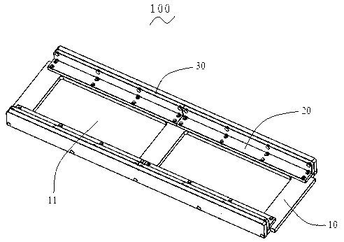
[0012] see figure 1 As shown, the splicing jig 100 of the present invention is used to fix a standard single crystal silicon assembled from two or more small single crystal silicon. The batching fixture 100 includes a base 10 , a support plate 20 mounted on the base 10 and a side wall 30 . The supporting boards 20 are located on two sides of the base 10 . The side wall 30 is mounted on the base 10 and located outside the support plate 20 . The side wall 30 is parallel to the support plate 20 . The base 10 is in the shape of a "day" and has two openings 11 on it.
[0013] When using the splicing jig 100 of the present invention, first place two or more small monocrystalline silicon in the splicing jig 100 and fix it, and then place the splicing...
PUM
 Abstract
Description
Claims
Application Information
 - R&D
- Intellectual Property
- Life Sciences
- Materials
- Tech Scout
- Unparalleled Data Quality
- Higher Quality Content
- 60% Fewer Hallucinations
Browse by: Latest US Patents, China's latest patents, Technical Efficacy Thesaurus, Application Domain, Technology Topic, Popular Technical Reports.
© 2025 PatSnap. All rights reserved.Legal|Privacy policy|Modern Slavery Act Transparency Statement|Sitemap|About US| Contact US: help@patsnap.com