Array substrate, display device and method for preparing array substrate

A technology of array substrates and mask plates, applied in static indicators, instruments, etc., can solve the problems of high design cost, poor production process compatibility, and high production cost, and achieve low production cost, strong production process compatibility, and structural differences small effect

Active Publication Date: 2015-12-02
BOE TECH GRP CO LTD +1
View PDF9 Cites 0 Cited by
  • Summary
  • Abstract
  • Description
  • Claims
  • Application Information

AI Technical Summary

Problems solved by technology

[0008] The internal structure of the GOA unit and the layout structure of the via holes are very different in the preparation process of the forward scanning array substrate and the reverse scanning array substrate. When the mask plate process is used for manufacturing, basically every mask The boards are not the same, which leads to problems such as poor compatibility of production process, high production cost and high design cost.

Method used


Image

  • Array substrate, display device and method for preparing array substrate
  • Array substrate, display device and method for preparing array substrate
  • Array substrate, display device and method for preparing array substrate

Examples


Embodiment 1

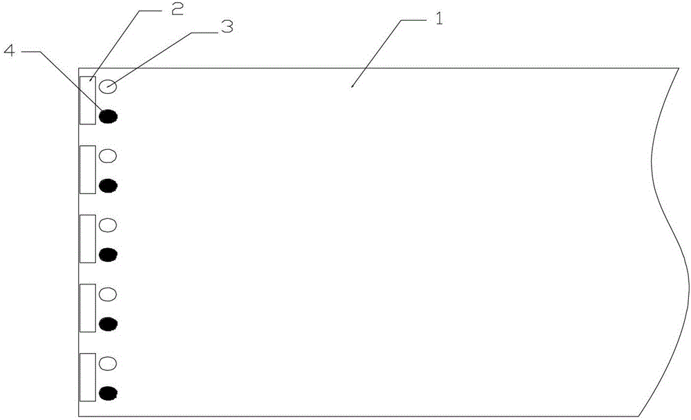
[0037] Such as figure 1 As shown, the array substrate 1 includes more than two gate drive GOA units 2 and vertical signal STV (Startvertical) signal lines; the transmission path between two adjacent GOA units 2 is formed by a via hole and a gate line metal layer or Composed of source and drain metal layers; the array substrate is provided with a pixel matrix, gate lines and data lines, and the GOA unit 2 is a drive unit that provides voltage to the gate lines connected to them in sequence; the previous GOA unit on the array substrate passes through the via hole connected to the metal layer of the gate line, and the latter GOA unit is also connected to the metal layer of the gate line through the via hole, and a transmission path is formed between the two GOA units. In the specific application process, the via hole can also be used to connect to the The source-drain metal layer forms a transmission path;

[0038] The array substrate is provided with a forward via area 3 and a ...

Embodiment 2

[0053] The display device of this embodiment includes the array substrate described in the first embodiment.

[0054] The display device may be a liquid crystal display device, including an array substrate and a color filter substrate disposed opposite to the array substrate, and the array substrate is a TFT-LCD array substrate. In a specific implementation process, the color filter substrate can also be replaced by a transparent substrate, and the color filter CF is arranged on the array substrate.

[0055] The display device may also be a box-type OLED display device, comprising an opposite substrate disposed opposite to the array substrate and an organic light-emitting material layer located between the array substrate and the opposite substrate.

[0056] The display device may be a display device using the array substrate, such as a liquid crystal television, electronic paper, and a flat panel.

Embodiment 3

[0058] The method for preparing the array substrate of this embodiment includes the step of setting a forward via area and a reverse via area;

[0059] in,

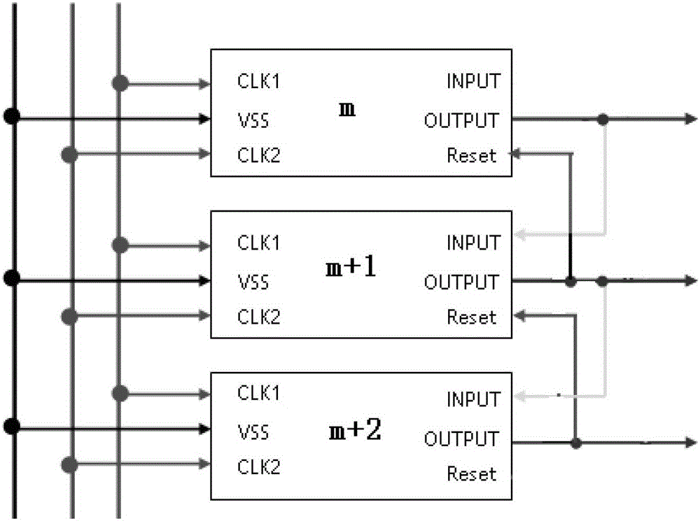
[0060] When the array substrate is scanning in the forward direction, the output end of the mth GOA unit and the input of the m+1th GOA unit are formed by setting the via hole mask process in the forward via hole area The forward via hole of the forward transmission path at the end, the first GOA unit is provided with a connection point connected to the STV signal line;

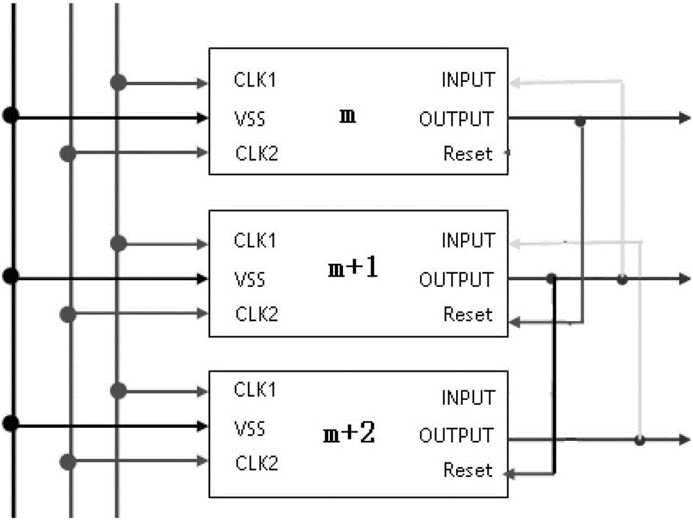
[0061] When the array substrate is scanned in the reverse direction, the output end of the m+1th GOA unit and the input of the mth GOA unit are connected in the reverse via hole area through the via hole mask process. The reverse via hole of the reverse transmission path at the end, and the last GOA unit is provided with a connection point connected to the STV signal line;

[0062] Wherein, the m=(1, 2, 3...M), M is the number of GOA units.

[0063] W...


PUM


Abstract

An array substrate, a display device, and a fabrication method of the array substrate. The array substrate comprises two or more GOA units (2) and an STV signal line. A transmission channel between two adjacent GOA units (2) is formed of a via hole and a gate line metal layer or a source / drain metal layer; a front-side via hole region (3) and a back-side via hole region (4) are provided on the array substrate, the front-side via hole region (3) is used to dispose a front-side via hole for forming a front-side transmission channel connecting an output end of the mth GOA unit (2) and an input end of the (m+1)th GOA unit (2), and the first GOA unit (2) is provided with a connecting point connected to the STV signal line; the back-side via hole region (4) is used to dispose a back-side via hole for forming a back-side transmission channel connecting an output end of the (m+1)th GOA unit (2) and an input end of the mth GOA unit (2), and the last GOA unit (2) is provided with a connecting point connected to the STV signal line, wherein m is an integer not less than 1. The array substrate is manufactured in low cost and has a desirable drive effect.

Description

technical field [0001] The present invention relates to the field of display, in particular to an array substrate, a display device and a method for preparing the array substrate. Background technique [0002] GOA——(GateDriverOnArray) Gate Driver on Array Substrate [0003] GOA technology integrates the gate drive on the array substrate, thereby omitting additional drivers such as flexible circuit thin film COF (ChipOnFilm) on the edge of the substrate, which is conducive to the miniaturization of the array substrate, and reduces the cost of materials and manufacturing. The cost of the process. [0004] One GOA unit corresponds to one gate line on the array substrate. Specifically, the output terminal of each GOA unit is connected to one gate line, and is also connected to the input terminal of the GOA unit connected to the next scanning gate line. [0005] There are two existing scanning methods: [0006] The first type: scan in the forward direction, that is, scan from ...

Claims


Application Information

Patent Timeline
Patent Type & Authority Patents(China)
IPC IPC(8): G09G3/20
CPCG09G3/3266
Inventor 马禹
Owner BOE TECH GRP CO LTD
Why Eureka
Try Eureka