Resistive variable memory based on vanadium oxide/alumina stack structure and its preparation method
A technology of resistive memory and stack structure, applied in the field of microelectronics, can solve the problem that the consistency of the intermediate state of the single-layer structure multi-value storage is difficult to be guaranteed, and achieve the effect of improving stability and consistency
- Summary
- Abstract
- Description
- Claims
- Application Information
AI Technical Summary
Problems solved by technology
Method used
Image
Examples
Embodiment 1
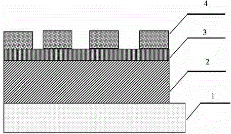
[0027] A resistive variable memory based on a vanadium oxide / alumina stack structure, such as figure 1 As shown, it consists of a copper lower electrode 1, a resistive layer and an aluminum upper electrode 4 and forms a laminated structure, wherein the resistive layer is a laminated structure of vanadium oxide film 3 and aluminum oxide film 4, and the thicknesses of each layer are: copper The lower electrode is 100 nm, the vanadium oxide film is 70 nm, the aluminum oxide film is 3 nm, and the aluminum upper electrode is 100 nm.
[0028] The preparation method of the resistive variable memory uses a silicon wafer as a substrate, first prepares a silicon dioxide insulating layer by thermal oxidation, and then prepares a 5 nm thick Ti paste on the silicon dioxide insulating layer by ion beam sputtering. Adhesive layer, and then prepare a low-power resistive variable memory on the Ti adhesive layer, the steps are as follows:
[0029] 1) On the Ti adhesion layer, the copper lower...
Embodiment 2
[0036] A resistive variable memory based on a vanadium oxide / alumina stack structure, such as figure 1 As shown, it consists of a copper lower electrode 1, a resistive layer and a platinum upper electrode 4 and forms a laminated structure, wherein the resistive layer is a laminated structure of vanadium oxide film 3 and aluminum oxide film 4, and the thicknesses of each layer are: copper The bottom electrode is 100 nm, the vanadium oxide film is 70 nm, the aluminum oxide film is 3 nm, and the platinum top electrode is 100 nm.
[0037] The preparation method of the resistive variable memory uses a silicon wafer as a substrate, first prepares a silicon dioxide insulating layer by thermal oxidation, and then prepares a 5 nm thick Ti paste on the silicon dioxide insulating layer by ion beam sputtering. Adhesive layer, and then prepare a low-power resistive variable memory on the Ti adhesive layer, the steps are as follows:
[0038] 1) Deposit a 100 nm Cu lower electrode on the T...
PUM
 Abstract
Description
Claims
Application Information


