A kind of preparation method of resistance type memory cell

A memory cell and resistive technology, applied in electrical components, circuits, electric solid-state devices, etc., can solve the problems of no stable intermediate state and difficulty in ensuring the consistency of multi-value storage, so as to improve storage density and stability, and realize stable Effects of Sex and Consistency

Inactive Publication Date: 2017-09-26
HENAN UNIV OF SCI & TECH
View PDF6 Cites 0 Cited by
  • Summary
  • Abstract
  • Description
  • Claims
  • Application Information

AI Technical Summary

Problems solved by technology

However, since the structure of the single-layer resistive variable layer determines that there is no stable intermediate state during the reset process, it is difficult to guarantee the consistency of the multi-value storage of the single-layer resistive variable layer structure.

Method used


Image

  • A kind of preparation method of resistance type memory cell
  • A kind of preparation method of resistance type memory cell
  • A kind of preparation method of resistance type memory cell

Examples


Embodiment 1

[0035] A preparation method of a resistive memory cell, the steps are as follows:

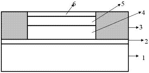
[0036] (1) The lower electrode layer is formed on the substrate by magnetron sputtering coating method: a metal Cu target is used, and Ar gas is used as the working gas to form a Cu thin film on the glass substrate by sputtering, and the working pressure during sputtering is 5 ×10 -1 Pa~10×10 - 1 Pa, the sputtering time is 20~25min, the sputtering voltage is 300~380V, the sputtering current is 120~180mA, and finally a Cu lower electrode layer with a thickness of about 80-150nm is formed on the glass substrate;

[0037] (2) Form an insulating dielectric layer on the Cu lower electrode layer: the method of forming the insulating dielectric layer can be atomic layer deposition or spin coating, and the thickness of the insulating dielectric layer is 300nm~5000nm. Material can be SiO 2 Or SiN, after the insulating dielectric layer is formed, a trench is formed on the insulating dielectric layer ...

Embodiment 2

[0042] A preparation method of a resistive memory cell, the steps are as follows:

[0043] (1) Use a metal Pt target, use Ar gas as the working gas, and form a Pt film on a semiconductor substrate by sputtering. The semiconductor substrate can be a Si substrate, and the working pressure during sputtering is 5×10 -1 Pa~10×10 -1 Pa, the sputtering time is 20~45min, the sputtering voltage is 300~380V, the sputtering current is 120~180mA, and a Pt lower electrode layer with a thickness of about 80-150nm is formed;

[0044] (2) Form an insulating dielectric layer on the Pt lower electrode layer. The method of forming the insulating dielectric layer can be deposition or spin coating. The thickness of the insulating dielectric layer is 300nm~5000nm. The material of the insulating dielectric layer can be SiO 2 Or SiN material, after forming the insulating dielectric layer, using a traditional photolithography process to form a trench on the insulating dielectric layer to form other ...


PUM


Abstract

A method for preparing a resistive memory unit, which relates to the technical field of nonvolatile memory devices. First, a lower electrode layer is formed on a substrate with a conductive material, and an insulating dielectric layer is deposited or spin-coated on the lower electrode layer. The process forms a trench on the insulating dielectric layer, and the bottom of the trench is connected to the lower electrode layer; then, the functional layer of the resistive memory unit is formed in the trench, and the functional layer is a stacked structure of upper and lower layers. It is composed of an amorphous SnOx layer and a oxynitride MnOxNy layer, and the range of x in the amorphous SnOx is 0

Description

technical field [0001] The invention relates to the technical field of nonvolatile memory devices, in particular to a method for preparing a resistive variable memory unit with a high-density film structure. Background technique [0002] In recent years, with the rapid development of computer technology and Internet technology, non-volatile memory devices have played an increasingly important role in the semiconductor industry. In a nonvolatile memory device, the basic cells of the device retain data stored in the basic cells even when power is cut off. Resistive Random Access Memory (RRAM) is a new type of non-volatile memory. Its working mechanism is to trigger a reversible resistance transition effect in an external electric field, that is, under the action of an applied voltage, the resistance of the device is in a low resistance state. ("0") and a high-resistance state ("1"), and the resulting resistance can be maintained after the external electric field is removed. ...

Claims


Application Information

Patent Timeline
Patent Type & Authority Patents(China)
IPC IPC(8): H01L45/00H01L27/24
Inventor 刘汇慧李同伟崔红玲毛爱霞王会娴
Owner HENAN UNIV OF SCI & TECH
Why Eureka
Try Eureka