Probe module for detecting contacting effect

A technology of probes and modules, which is applied in the field of probe modules, can solve problems such as long time consumption, small current, and complex abnormal handling of equipment, so as to achieve the effect of simple finding and solving abnormal situations and eliminating the time spent on cause finding and processing

Active Publication Date: 2013-09-25
TCL CHINA STAR OPTOELECTRONICS TECH CO LTD
View PDF4 Cites 16 Cited by
  • Summary
  • Abstract
  • Description
  • Claims
  • Application Information

AI Technical Summary

Problems solved by technology

[0009] However, there are many situations at present. When the monitored current value is too large, it can be basically determined that the probe is in good contact. It is due to other reasons such as an internal short circuit of the LCD panel that the current is abnormally large.
However, when the current is too small, it may be caused by poor contact of the probe, which may cause the current to be too small. It may also be that the internal circuit of the LCD panel is disconnected, or a part of the circuit is disconnected, resulting in an increase in resistance and a decrease in the current. Therefore, it is impossible to quickly confirm whether it is due to a probe contact problem. Causes an exception, making device exception handling complicated and time-consuming

Method used


Image

  • Probe module for detecting contacting effect
  • Probe module for detecting contacting effect
  • Probe module for detecting contacting effect

Examples


Embodiment Construction

[0029] In order to make the object, technical solution and advantages of the present invention clearer, the present invention will be further described in detail below in conjunction with the accompanying drawings.

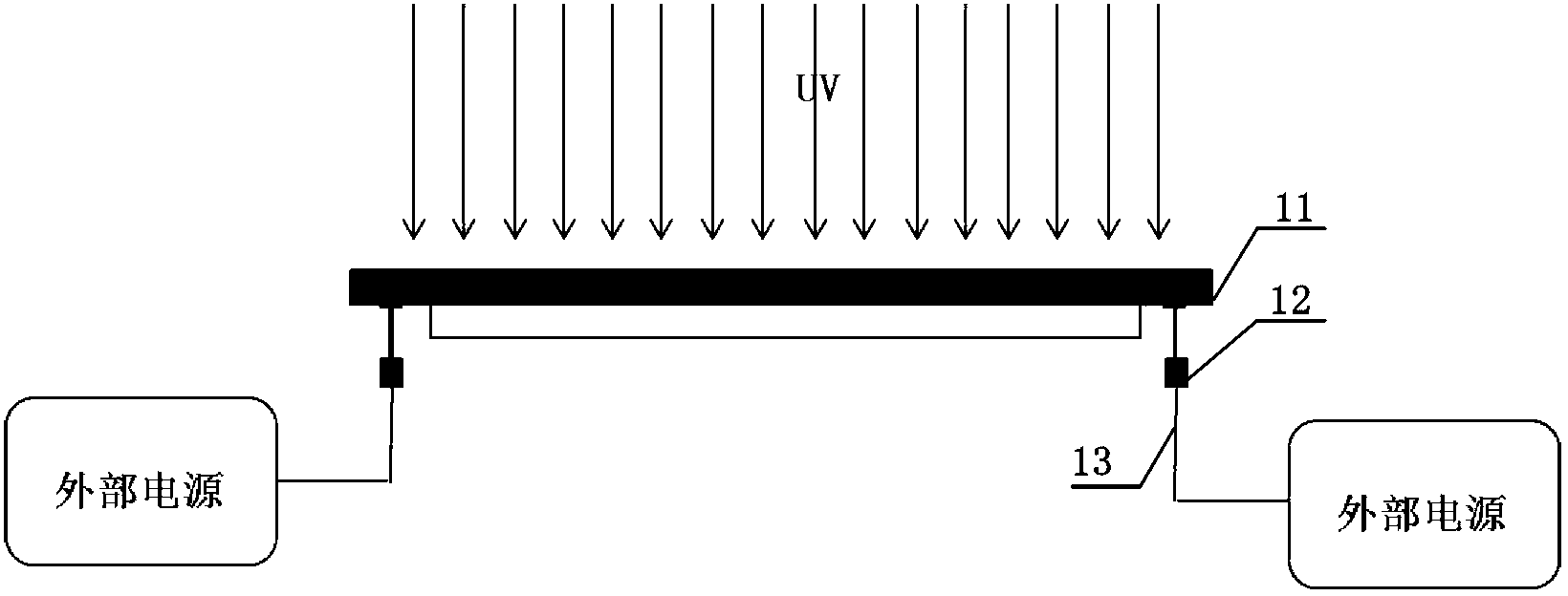
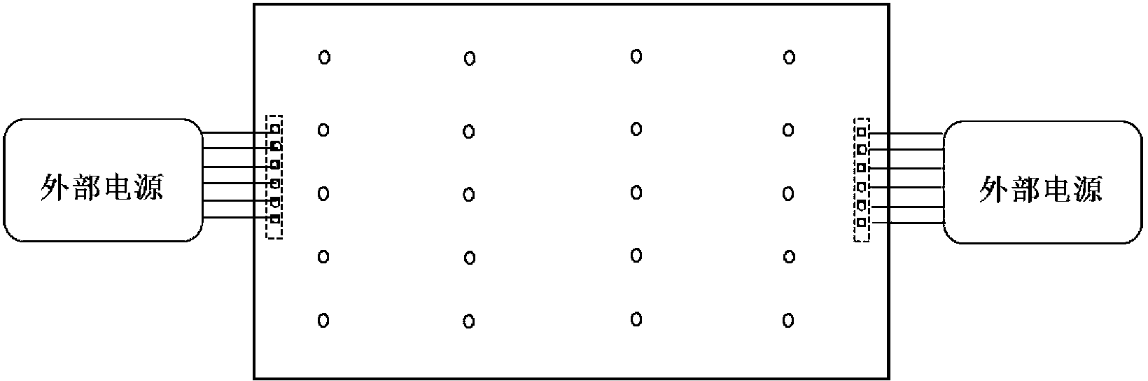
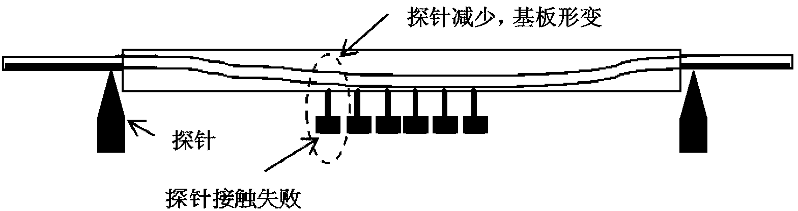
[0030] Image 6 is a schematic structural diagram of a probe module according to an embodiment of the present invention. During the liquid crystal alignment process, the probe module can independently monitor the contact effect between the probe itself and the external test circuit of the substrate, and determine the contact effect in time.

[0031] like Image 6 As shown, the probe module includes two mutually insulated retractable probes, an external power supply electrically connected to one of the retractable probes through a signal line 51, and a resistor electrically connected to the other retractable probe. The monitoring device 63 is electrically connected to an external power source, and the alarm device 43 is electrically connected to the resistance mo...


PUM


Abstract

The invention discloses a probe module for detecting a contacting effect. In the process of liquid crystal alignment, the probe module is used for detecting the contacting effect of the probe module self and a substrate external test circuit of an LCD panel. The probe module for detecting the contacting effect comprises at least two telescopic probes and a resistance monitoring device, wherein the at least two telescopic probes are mutually insulated, the resistance monitoring device is electrically connected with the at least two mutually-insulated telescopic probes, and the resistance monitoring device monitors the resistance between the at least two mutually-insulated telescopic probes to judge the contacting effect of the at least two mutually-insulated telescopic probes and a contact surface. According to the probe module for detecting the contacting effect, due to the facts that a plurality of contact points are formed between the probe module and a contact object and the contact points are in mutual independence, the resistance monitoring device of the probe module is used so that the resistance values among a plurality of probes obtained through measurement can be used for timely judging the contacting effect between the probes and the contact object, and thus cause seeking and handling time due to abnormal monitoring currents in an existing liquid crystal alignment process is saved.

Description

technical field [0001] The invention relates to the technical field of liquid crystal display manufacturing, in particular to a probe module used for detecting contact effects during liquid crystal alignment. Background technique [0002] In recent years, with the thinner display trend, Liquid Crystal Display (LCD for short) has been widely used in various electronic products, such as mobile phones, notebook computers, and color TV sets. [0003] During the manufacturing process of the liquid crystal panel, initial alignment of the liquid crystal is required. At present, ultraviolet curing (UV Curing for short) is an important process for aligning liquid crystals. This method mainly completes the alignment of liquid crystals through the joint action of UV and electric field after the liquid crystal panel is filled with liquid crystals. [0004] When performing UV Curing liquid crystal alignment, an electric field is applied to the liquid crystal, and then UV irradiation is ...

Claims


Application Information

Patent Timeline
Patent Type & Authority Applications(China)
IPC IPC(8): G01R1/073G02F1/13G02F1/1337
CPCG01R1/07314G09G3/006G01R1/06794
Inventor 宋涛赵国栋刘明马涛
Owner TCL CHINA STAR OPTOELECTRONICS TECH CO LTD
Why Eureka
Try Eureka