Power semiconductor chip and manufacturing method thereof

A technology of power semiconductors and chips, which is applied in semiconductor/solid-state device manufacturing, semiconductor devices, electrical components, etc., can solve problems such as uneven current between cells, uneven current, and switching speed differences, and achieve improved current sharing characteristics, improving the habit of current sharing, and improving the effect of switching control ability

Active Publication Date: 2013-09-25
ZHUZHOU CRRC TIMES SEMICON CO LTD
View PDF5 Cites 5 Cited by
  • Summary
  • Abstract
  • Description
  • Claims
  • Application Information

AI Technical Summary

Problems solved by technology

Although this method can improve chip-level current sharing to a certain extent, it cannot fundamentally solve the problem of uneven current sharing.
This is because a chip is composed of tens of thousands of cells connected in parallel, and only one gate resistor is connected in series inside the chip. There are still differences in the switching speed between cells, and there are still differences between cells. current sharing

Method used


Image

  • Power semiconductor chip and manufacturing method thereof
  • Power semiconductor chip and manufacturing method thereof
  • Power semiconductor chip and manufacturing method thereof

Examples


Embodiment 1

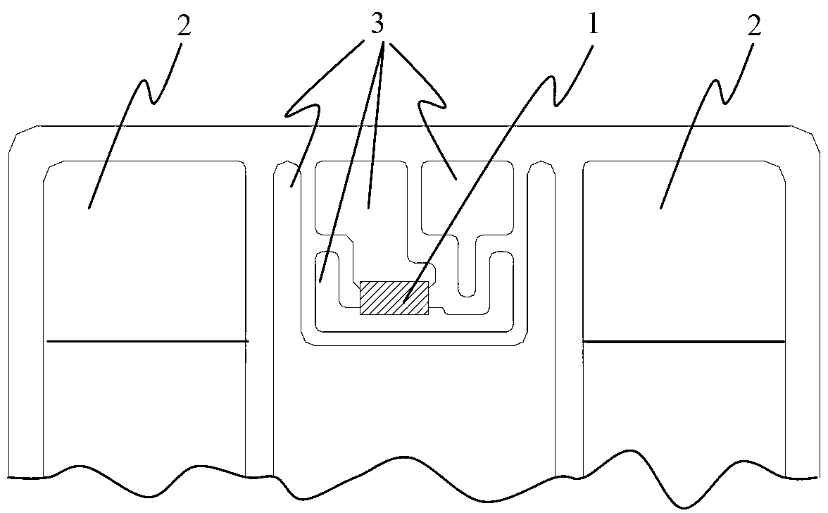
[0056] combine figure 2 The structure of the cell unit of the power semiconductor chip provided by the embodiment of the present invention will be described in detail. figure 2 It is a schematic cross-sectional structure diagram of a cell unit of a power semiconductor chip provided by an embodiment of the present invention.

[0057] Such as figure 2 As shown, a cell unit of the power semiconductor chip includes a substrate 100 provided with a semiconductor structure; the front side of the substrate 100 includes a first sub-surface S1, a second sub-surface S2 and a third sub-surface S3, wherein the third The sub-surface S3 is the area where the center of the front surface is located, the second sub-surface S2 surrounds the third sub-surface, the first sub-surface S1 is located at the outermost periphery of the cell unit, and the first sub-surface S1 surrounds the second sub-surface S2 and the second sub-surface S2. The three sub-surfaces S3, the specific positional relatio...

Embodiment 2

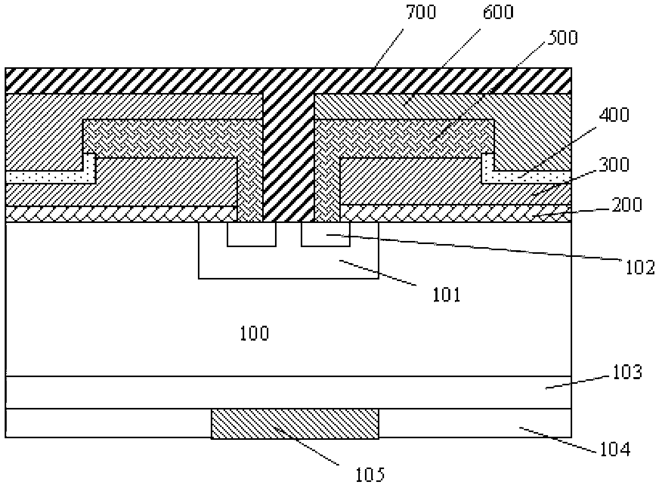
[0087] combine Figure 5 6 (9) to describe the preparation method of the power semiconductor chip. Such as Figure 5 As shown, the preparation method of the power semiconductor chip comprises the following steps,

[0088] S51. Provide a substrate provided with a semiconductor structure:

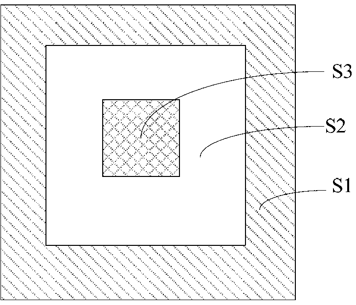
[0089] Such as image 3 as shown, image 3 is the front top view of the substrate. The substrate front side has a first subsurface, a second subsurface, and a third subsurface. The positional relationship of the first sub-surface, the first sub-surface, the second sub-surface and the third sub-surface is the same as that of the sub-surfaces on the substrate described in the first embodiment above. For the sake of brevity, no detailed description is given here, please refer to the corresponding part of Embodiment 1.

[0090] As shown in FIG. 6(1), a semiconductor structure corresponding to the power semiconductor chip is disposed inside the substrate. The semiconductor structure includ...


PUM


Abstract

The invention provides a power semiconductor chip and a manufacturing method thereof. The power semiconductor chip is formed by parallel connection of N cellular elements, wherein at least one cellular element comprises a metal silicide layer located on the periphery of the cellular element, each metal silicide layer is at least located above the peripheral area of a polycrystalline silicon layer of a corresponding cellular element, the metal silicide layers can serve as gate resistors functionally, the gate resistors surround the cellular elements of the chip to achieve cellular element based parallel connection of the gate resistors, cellular element based switch control capacity is improved, and flow equalizing property of the chip is improved.

Description

technical field [0001] The invention relates to the field of semiconductor devices, in particular to a power semiconductor chip and a preparation method thereof. Background technique [0002] In many application fields of power electronic devices, many power semiconductor chips (such as IGBT, MOSFET, etc.) are often connected in parallel to achieve the target power level. The parallel application of power semiconductor chips is very common, including the parallel connection of module level, substrate level and chip level. In addition, tens of thousands of cells inside each chip are also arranged in parallel. For each repeating unit connected in parallel, making it have a uniform current and the same switching speed is the best protection measure and the means to improve reliability. [0003] Currently, the most commonly used method is the figure 1 As shown, the grid resistor is connected in series on the substrate or substrate to control the switching speed of the substra...

Claims


Application Information

Patent Timeline
Patent Type & Authority Applications(China)
IPC IPC(8): H01L29/78H01L29/739H01L21/336H01L21/331
Inventor 刘国友覃荣震黄建伟罗海辉
Owner ZHUZHOU CRRC TIMES SEMICON CO LTD
Why Eureka
Try Eureka