A power semiconductor chip gate region

A technology of power semiconductors and gate regions, which is applied in semiconductor devices, electrical components, circuits, etc., can solve the problems of uneven switching speed, uneven current, and large signal differences between chips, so as to improve the uniformity of switching speed, The effect of reducing error sensitivity

Active Publication Date: 2015-09-23
ZHUZHOU CRRC TIMES SEMICON CO LTD
View PDF5 Cites 0 Cited by
  • Summary
  • Abstract
  • Description
  • Claims
  • Application Information

AI Technical Summary

Problems solved by technology

Since the error of the resistance value of a single resistor is generally large, for the same gate pad area signal between different chips, the signal on the gate bus bar is very different, which easily leads to uneven switching speed and uneven current technology between chips. question

Method used


Image

  • A power semiconductor chip gate region
  • A power semiconductor chip gate region
  • A power semiconductor chip gate region

Examples


Embodiment Construction

[0024] The present invention will be described in detail below in conjunction with specific embodiments shown in the accompanying drawings. However, these embodiments do not limit the present invention, and any structural, method or functional changes made by those skilled in the art according to these embodiments are included in the protection scope of the present invention.

[0025] Furthermore, repeated reference numerals or designations may be used in different embodiments. These repetitions are only for the purpose of simply and clearly describing the present invention, and do not represent any relationship between the different embodiments and / or structures discussed.

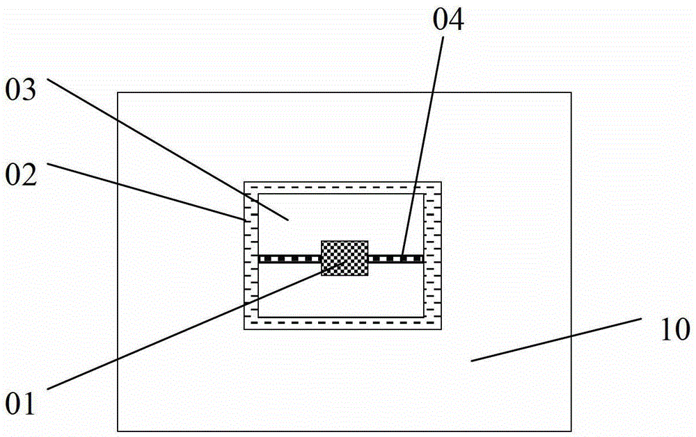
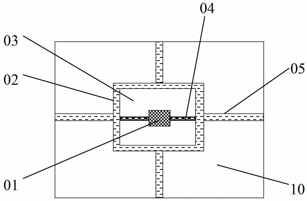
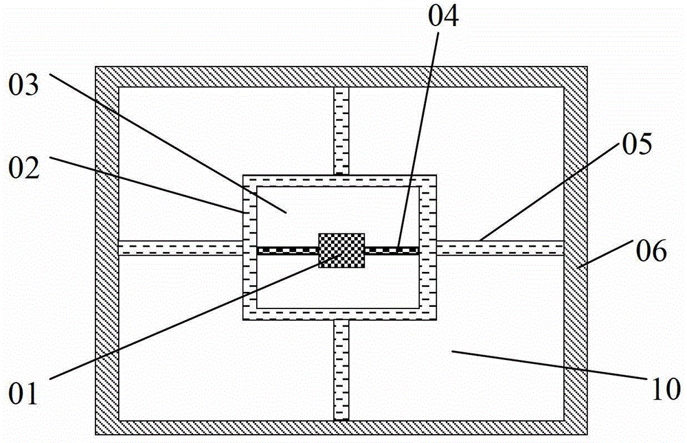
[0026] see figure 1 The gate area structure of the power semiconductor chip provided by the embodiment of the present invention includes a main gate area 01 located near the center of the chip cell area 10, a first gate bar 02 surrounding the main gate area 01, and a main gate area located in the main g...


PUM


Abstract

The invention provides a gate region of a power semiconductor chip, which comprises a main gate region, a first grid strip and a gate resistance region, wherein the main gate region is positioned in a chip cellular area; the first grid strip surrounds the main gate region; the gate resistance area is positioned between the main gate region and the first grid strip; at least two sub-resistances are connected in parallel in the gate resistance area; one end of each sub-resistance is connected with the main gate region; the other end of each sub-resistance is connected with the first grid strip. The gate region structure avoids the risk that the entire chip can not work normally or is damaged due to damage of one gate resistance. In addition, the structure that a plurality of resistances are connected in parallel is adopted to greatly reduce huge changes of resistance value of the resistance due to the error of the gate resistance, so that uniformity of the switching speed between two chips and the uniform current distribution property between two chips are ensured.

Description

technical field [0001] The invention relates to the field of semiconductor devices, in particular to a gate region of a power semiconductor chip. Background technique [0002] At present, the gate region structure of power semiconductor chips such as IGBT, MOSFET, etc. in the prior art includes two parts, the gate pad region and the gate bus bar, wherein the gate pad region and the gate bus bar are electrically connected through a series resistor. The structure of the gate region has the following disadvantages: [0003] First, when the resistance connected in series between the gate pad area and the gate bus bar is damaged, the gate pad area and the bus bar cannot be connected, which affects the normal operation of the chip and even causes damage to the chip. [0004] Secondly, in many application fields of power electronic devices, multiple power semiconductor chips are often connected in parallel to achieve the target power level. The multiple power semiconductor chips ...

Claims


Application Information

Patent Timeline
Patent Type & Authority Patents(China)
IPC IPC(8): H01L29/423
Inventor 刘国友覃荣震黄建伟罗海辉
Owner ZHUZHOU CRRC TIMES SEMICON CO LTD
Why Eureka
Try Eureka