Supercharge Your Innovation With Domain-Expert AI Agents!

Manufacturing method of wiring board and wiring board

A technology of wiring substrate and manufacturing method, applied in the directions of printed circuit manufacturing, multilayer circuit manufacturing, insulating substrate/layer processing, etc., can solve problems such as poor connection between wiring substrate and semiconductor device, and achieve the effect of reducing poor connection

Active Publication Date: 2017-09-22
SHINKO ELECTRIC IND CO LTD
View PDF1 Cites 0 Cited by
  • Summary
  • Abstract
  • Description
  • Claims
  • Application Information

AI Technical Summary

Problems solved by technology

That is, it causes poor connection between the wiring board and the semiconductor device.

Method used


Image

  • Manufacturing method of wiring board and wiring board
  • Manufacturing method of wiring board and wiring board
  • Manufacturing method of wiring board and wiring board

Examples


Embodiment Construction

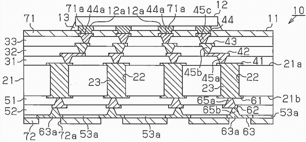
[0016] One embodiment will be described below with reference to the drawings. In addition, the drawings are for explaining a schematic structure, and do not show actual sizes and ratios.

[0017] Such as figure 1 As shown, the semiconductor device 10 (semiconductor package) includes a wiring substrate 11 and a surface mounted on the wiring substrate 11 ( figure 1 The semiconductor chip 12 on the upper surface). The wiring substrate 11 includes a core substrate 21 . For example, the core substrate 21 is a so-called glass epoxy substrate formed by curing a thermosetting insulating resin containing epoxy resin as a main component impregnated with glass fiber cloth (glass woven cloth) as a reinforcing material.

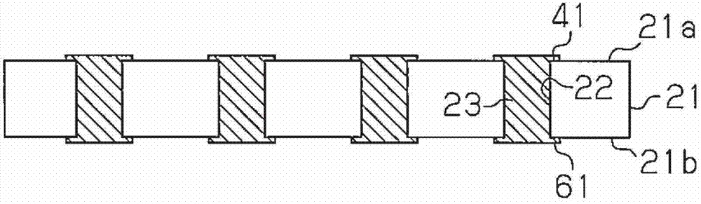
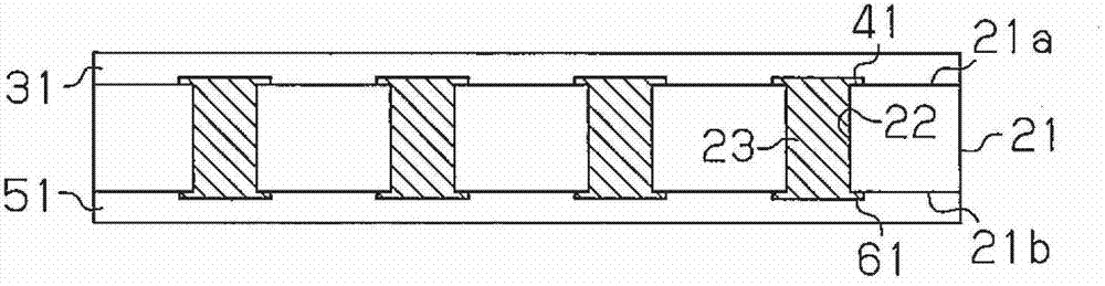
[0018] The core substrate 21 includes a first surface ( figure 1 The upper surface 21a) and the second surface on the opposite side of the first surface ( figure 1 In the lower surface 21b). A plurality of through holes 22 penetrating between the upper surface 21 a ...


PUM


Abstract

A method for manufacturing a wiring substrate includes alternately stacking first wiring patterns and first insulative layers on a first surface of a core substrate and alternately stacking second wiring patterns and second insulative layers on a second surface of the core substrate at an opposite side of the first surface. The number of the second insulative layers excluding the outermost second insulative layer differs from the number of the first insulative layers. The method further includes forming a via hole in the outermost first insulative layer to expose a portion of the outermost first wiring pattern, and exposing the outermost second wiring pattern by reducing the outermost second insulative layer in thickness. The method further includes forming a via in the via hole and forming a wiring pattern, which is connected by the via to the outermost first wiring pattern, on the outermost first insulative layer.

Description

technical field [0001] The present invention relates to a method of manufacturing a wiring board and a wiring board. Background technique [0002] Japanese Patent Application Laid-Open No. 9-321434 describes a conventional example of a multilayer wiring board used for mounting electronic components. The multilayer wiring board has a plurality of insulating layers and a plurality of wiring layers arranged on both surfaces of the core substrate. In such a wiring board, for example, the same number of insulating layers and wiring layers are provided on each surface of the core board. A protective film is formed on the upper surface of the wiring board, and a part of the wiring pattern exposed from the opening of the protective film is used as an electrode for connecting electronic components such as a semiconductor device (LSI). A part of the wiring pattern exposed from the opening of the protective film formed on the lower surface of the wiring board is used as an electrode ...

Claims


Application Information

Patent Timeline
Patent Type & Authority Patents(China)
IPC IPC(8): H05K3/46H01L21/48H01L23/498H05K1/00
CPCH01L21/486H01L23/145H01L23/15H01L23/49827H01L23/49894H01L2224/16H01L2224/73204H05K1/0271H05K3/0055H05K3/4644H05K3/4673H05K2201/09781H05K2201/09881Y10T29/49128H05K1/0298
Inventor 堀内章夫
Owner SHINKO ELECTRIC IND CO LTD
Features
  • R&D
  • Intellectual Property
  • Life Sciences
  • Materials
  • Tech Scout
  • Unparalleled Data Quality
  • Higher Quality Content
  • 60% Fewer Hallucinations
Learn More