Array substrate and liquid crystal display panel
A technology of array substrates and thin film transistors, applied in static indicators, instruments, nonlinear optics, etc., can solve the problems of inability to achieve LCS effects, color distortion, etc., reduce color distortion, reduce color differences, and increase aperture ratio Effect
- Summary
- Abstract
- Description
- Claims
- Application Information
AI Technical Summary
Problems solved by technology
Method used
Image
Examples
Embodiment Construction
[0021] The present invention will be described in detail below in conjunction with the embodiments and the accompanying drawings.
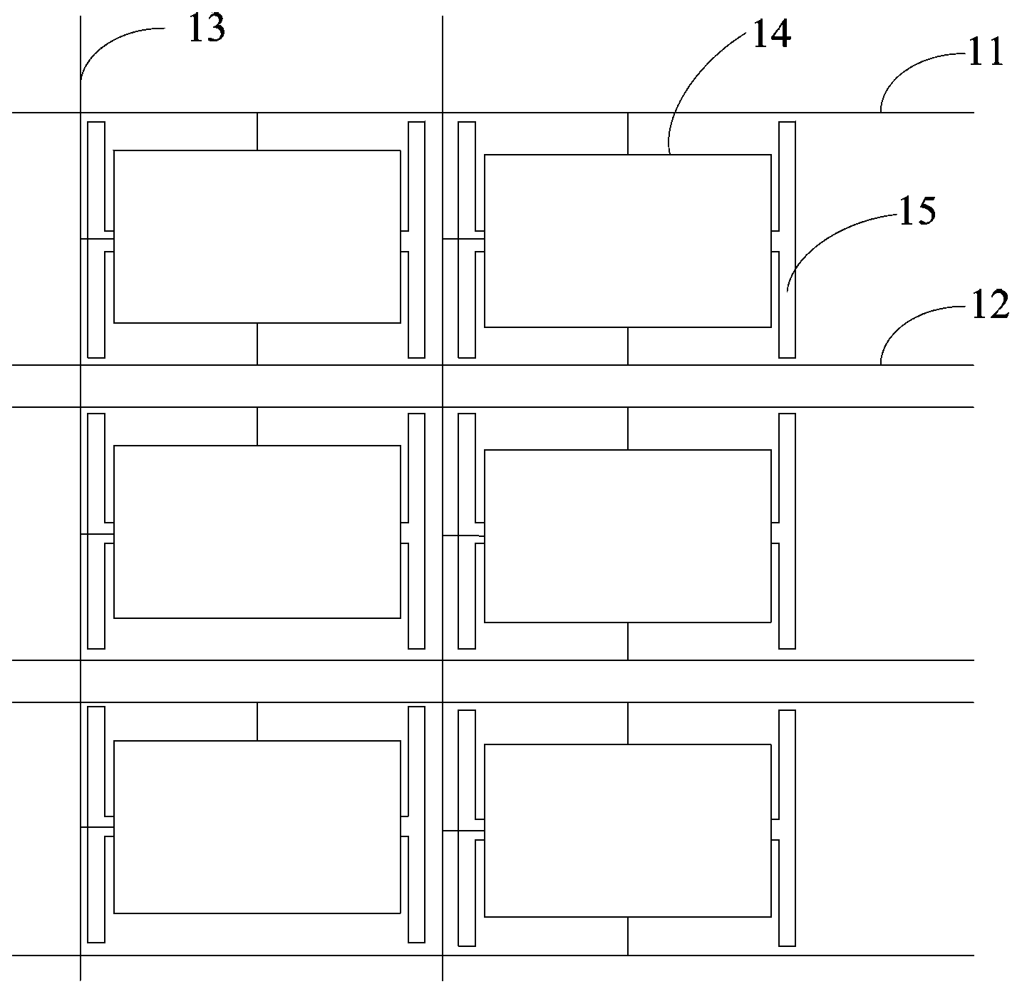
[0022] refer to figure 1In one embodiment of the array substrate of the present invention, the array substrate includes a plurality of first scan lines 11, a plurality of second scan lines 12, a plurality of data lines 13, a plurality of pixel units 14, and a common electrode for inputting a common voltage 15. A plurality of pixel units 14 are arranged in an array, and each pixel unit 14 is connected to a first scan line 11 , a second scan line 12 and a data line 13 .
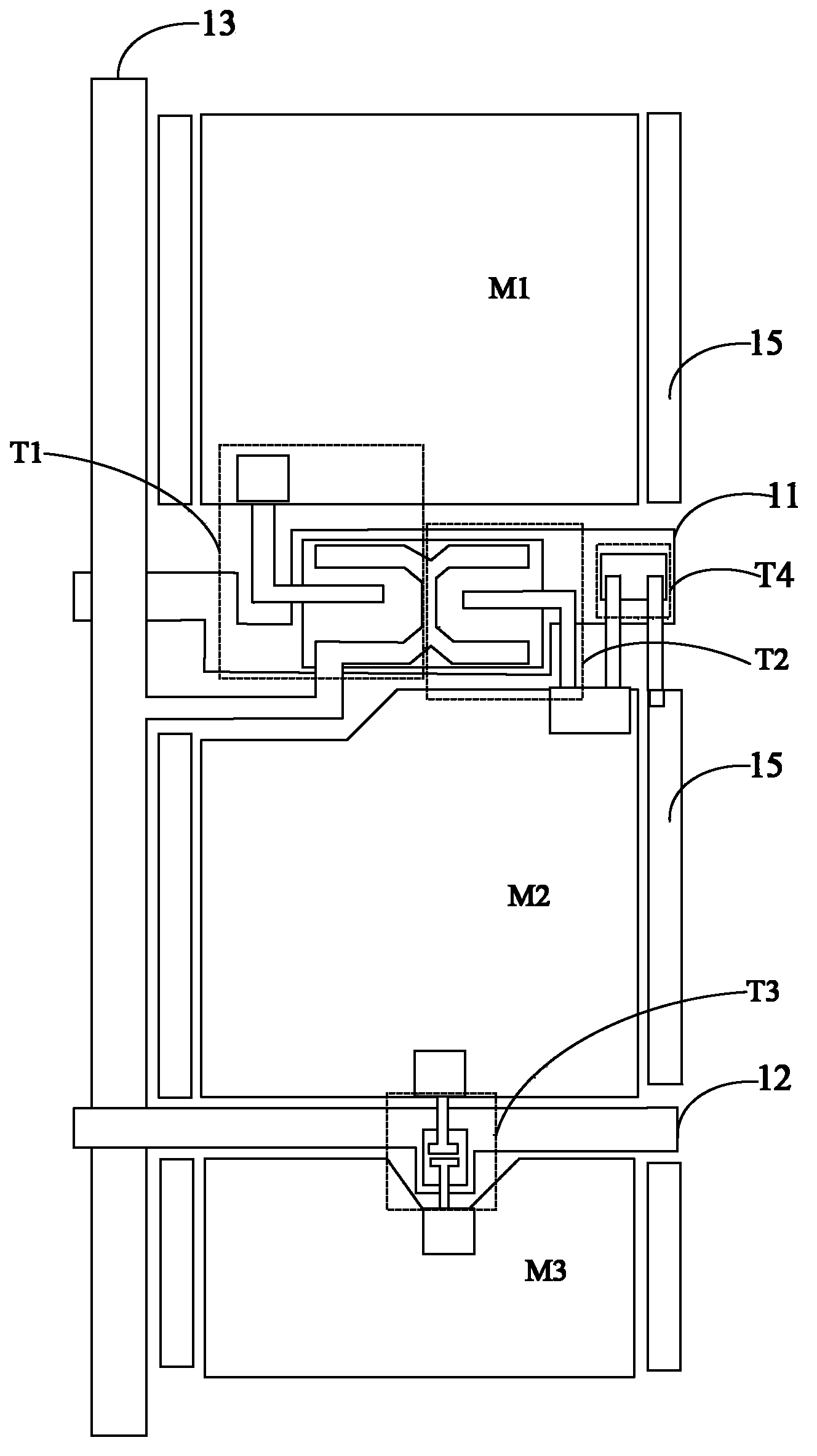
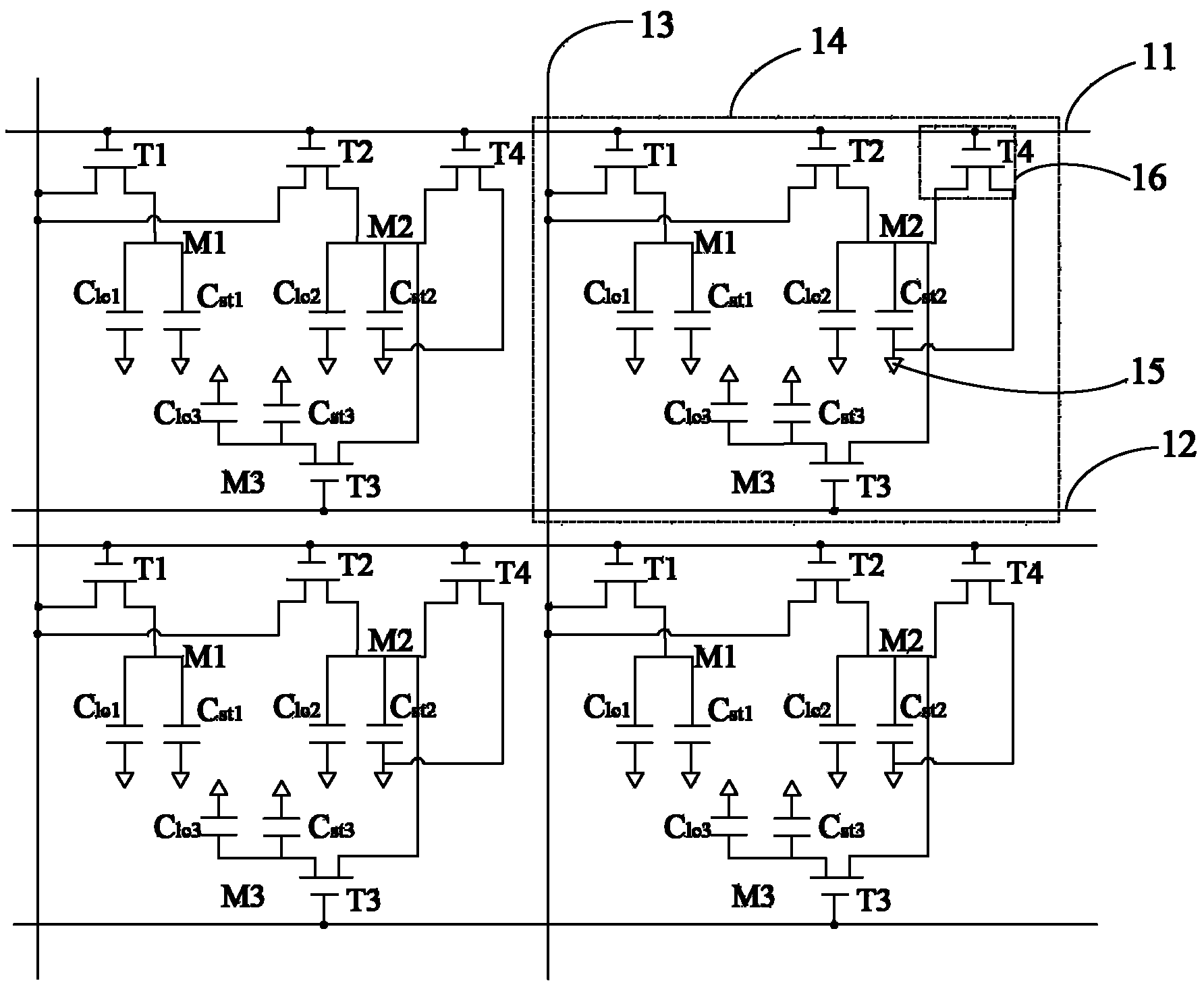
[0023] which, combined with figure 2 and image 3 , each pixel unit 14 includes a first pixel electrode M1, a second pixel electrode M2, a third pixel electrode M2, and a first switch respectively acting on the first pixel electrode M1, the second pixel electrode M2, and the third pixel electrode M3 T1, the second switch T2 and the third switch T3. The control terminal of the...
PUM
 Abstract
Description
Claims
Application Information


