A high gain boost circuit

A high-gain, circuit technology, applied in electrical components, adjusting electrical variables, instruments, etc., can solve problems such as system collapse, system stability degradation, and increased number of switching tubes

Active Publication Date: 2016-04-13
SOUTH CHINA UNIV OF TECH
View PDF4 Cites 0 Cited by
  • Summary
  • Abstract
  • Description
  • Claims
  • Application Information

AI Technical Summary

Problems solved by technology

The traditional Boost circuit can no longer meet the needs of the industry, and the industry needs a higher gain boost circuit
The traditional method is to cascade boost through multiple Boost link circuits. This method is costly, and due to the increase in the number of switch tubes, the stability of the system will decrease. If one of the links crashes, the entire system will collapse.

Method used


Image

  • A high gain boost circuit
  • A high gain boost circuit
  • A high gain boost circuit

Examples


Embodiment

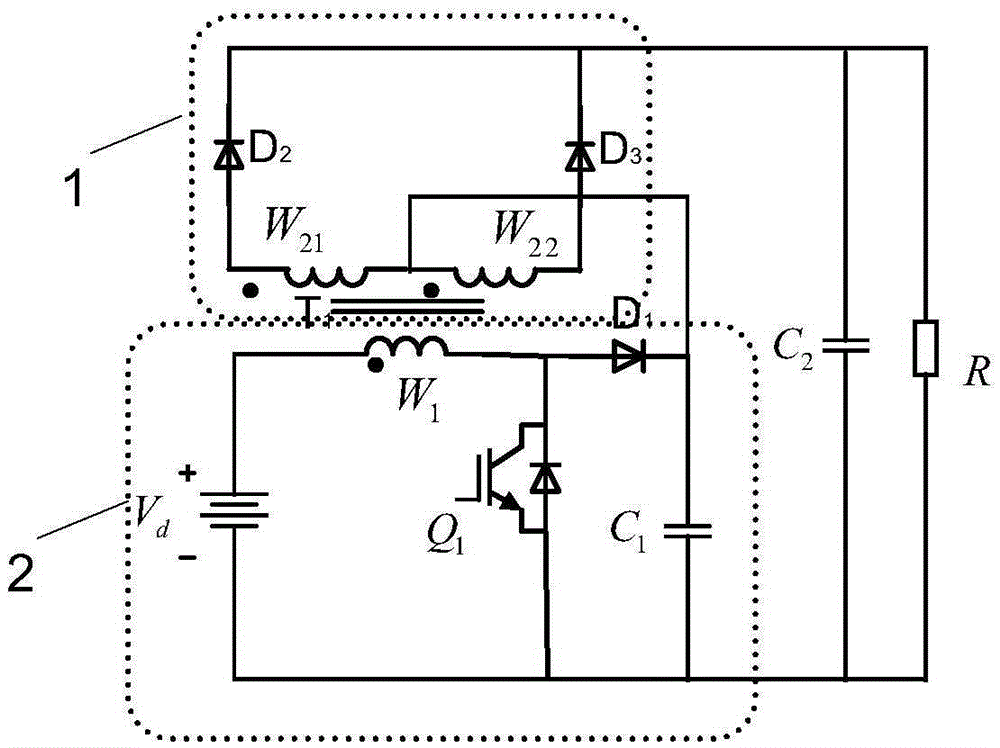
[0025] Such as figure 1 As shown, a high-gain Boost circuit includes a transformer T 1 , switch tube Q 1 , the first diode D 1 , the second diode D 2 , the third diode D 3 , the first energy storage capacitor C 1 , the second energy storage capacitor C 2 and load R;

[0026] The transformer T 1 The first secondary winding W 21 , the second secondary winding W 22 , the second diode D 2 and the third diode D 3 Constitute a transformer step-up module 1;

[0027] The transformer T 1 The primary winding W 1 , switch tube Q 1 , the first diode D 1 and the first storage capacitor C 1 Constitute Boost circuit module 2;

[0028] The second storage capacitor C 2 And the load R constitutes the output module.

[0029] Specific connection:

[0030] The DC power supply V d The positive pole of the transformer T 1 The primary winding W 1 The end connection of the same name;

[0031] The transformer T 1 The primary winding W 1 The opposite end, the first diode D 1 T...


PUM


Abstract

The invention discloses a high-grain Boost circuit, which comprises a transformer (T1), a switch tube (Q1), a first diode (D1), a second diode (D2), a third diode (D3), a first energy storage capacitor (C1), a second energy storage capacitor (C2) and a load (R), wherein a first secondary winding (W21), a second secondary winding (W22), a second diode (D2) and a third diode (D3) of the transformer (T1) form a transformer boosting module (1), and a primary winding (W1), the switch tube (Q1), the first diode (D1) and the first energy storage capacitor (C1) of the transformer (T1) form an output module. The high-grain Boost circuit solves the problem that the stability of the system is degraded as the number of the switch tubes is increased.

Description

technical field [0001] The invention relates to the technical field of power electronic circuits, in particular to a high-gain Boost circuit. Background technique [0002] With the development of life and industry, the requirements for power electronic circuits are becoming increasingly stringent. The traditional boost circuit can no longer meet the needs of the industry, and the industry needs a higher gain boost circuit. The traditional method is to cascade boost through multiple Boost link circuits. This method is costly and due to the increase in the number of switch tubes, the stability of the system is reduced. If one of the links fails, the entire system will collapse. Contents of the invention [0003] In order to overcome the shortcomings and deficiencies of the prior art, the present invention provides a high-gain Boost circuit, which is suitable for power electronic circuits requiring high gain. [0004] The technical scheme adopted in the present invention: ...

Claims


Application Information

Patent Timeline
Patent Type & Authority Patents(China)
IPC IPC(8): H02M3/335
Inventor 张波张桂东
Owner SOUTH CHINA UNIV OF TECH
Why Eureka
Try Eureka