Thin film transistor, array substrate, display device and manufacturing method of thin film transistor

A technology of thin film transistors and array substrates, which is applied in the fields of thin film transistors, display devices, array substrates, and thin film transistors. It can solve problems affecting display quality, etc., and achieve solutions to Schottky resistance, reduced contact resistance, and high conductivity. Effect

Inactive Publication Date: 2018-11-30
BOE TECH GRP CO LTD
View PDF7 Cites 0 Cited by
  • Summary
  • Abstract
  • Description
  • Claims
  • Application Information

AI Technical Summary

Problems solved by technology

[0004] In order to solve the problem that the annealed metal oxide film and the drain-source contact produce Schottky resistance and affect the display quality, an embodiment of the present invention provides a thin film transistor, an array substrate, a display device, and a thin film transistor manufacturing method

Method used


Image

  • Thin film transistor, array substrate, display device and manufacturing method of thin film transistor
  • Thin film transistor, array substrate, display device and manufacturing method of thin film transistor
  • Thin film transistor, array substrate, display device and manufacturing method of thin film transistor

Examples


Embodiment Construction

[0041] In order to make the object, technical solution and advantages of the present invention clearer, the implementation manner of the present invention will be further described in detail below in conjunction with the accompanying drawings.

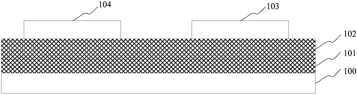
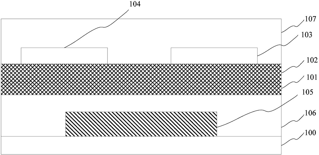
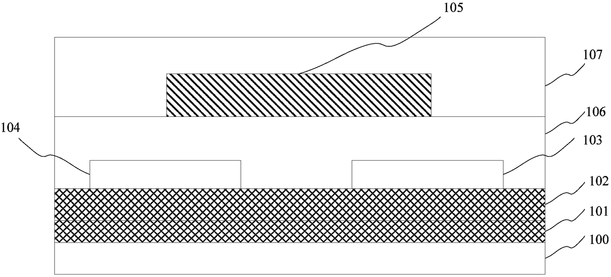
[0042] figure 1 is a schematic structural diagram of a thin film transistor provided by an embodiment of the present invention, see figure 1 , the thin film transistor includes: a substrate 100, a first metal oxide thin film layer 101 disposed on the substrate 100 and subjected to annealing treatment, a second metal oxide thin film disposed on the first metal oxide thin film layer 101 without annealing treatment layer 102 and a source electrode 103 and a drain electrode 104 disposed on the second metal oxide thin film layer 102 .

[0043] The thin film transistor of the present invention includes the annealed first metal oxide thin film layer 101, and the annealing treatment eliminates excessive oxygen vacancies in the metal oxide, so...


PUM

PropertyMeasurementUnit
thicknessaaaaaaaaaa
thicknessaaaaaaaaaa
thicknessaaaaaaaaaa

Abstract

The invention discloses a thin film transistor, an array substrate, a display device, and a thin film transistor making method, belonging to the technical field of display. The thin film transistor comprises a substrate, a first metal oxide film layer which is arranged on the substrate and annealed, a second metal oxide film layer which is arranged on the first metal oxide film layer and not annealed, and a source electrode and a drain electrode which are arranged on the second metal oxide film layer. The problem that annealed metal oxide contacts the drain and the source to generate Schottky resistance and thus causes a decrease in stability of the thin film transistor is solved.

Description

technical field [0001] The invention relates to the field of display technology, in particular to a thin film transistor, an array substrate, a display device and a manufacturing method of the thin film transistor. Background technique [0002] Metal oxide thin film transistors are currently a research hotspot in the field of thin film transistors, such as indium gallium zinc oxide IGZO thin film transistors. [0003] A metal oxide thin film transistor generally includes a substrate, a metal oxide thin film (active layer) disposed on the substrate, and drain-source electrodes (drain electrode and source electrode). In metal oxide thin film transistors, oxygen vacancies are the main source of carriers, but too much oxygen vacancies will lead to the increase of defect states in metal oxide thin films, which will affect the carrier density, mobility and semiconductor reliability. In order to solve the problem of increasing defect states inside the metal oxide film caused by ox...

Claims


Application Information

Patent Timeline
Patent Type & Authority Patents(China)
IPC IPC(8): H01L21/77H01L27/12H01L29/786
CPCH01L21/77H01L27/1214H01L27/1259H01L29/78603
Inventor 黎午升曹占锋
Owner BOE TECH GRP CO LTD
Why Eureka
Try Eureka