Liquid crystal display (LCD) screen and display device

A liquid crystal display and liquid crystal layer technology, applied in optics, instruments, nonlinear optics, etc., can solve the problem of reducing the aperture ratio of the pixel unit of the liquid crystal display, and achieve the effect of improving viewability and enhancing display brightness

Active Publication Date: 2013-11-27
BEIJING BOE OPTOELECTRONCIS TECH CO LTD
View PDF5 Cites 47 Cited by
  • Summary
  • Abstract
  • Description
  • Claims
  • Application Information

AI Technical Summary

Problems solved by technology

However, the use of transflective will reduce the aperture ratio of each pixel unit in the liquid crystal display

Method used


Image

  • Liquid crystal display (LCD) screen and display device
  • Liquid crystal display (LCD) screen and display device
  • Liquid crystal display (LCD) screen and display device

Examples


example 1

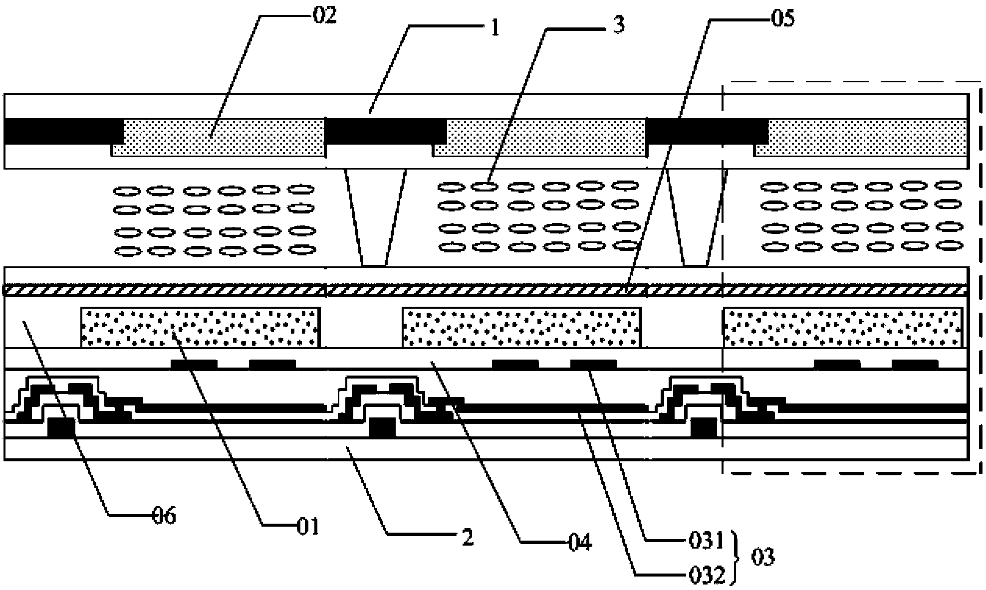
[0048] The color filter 02 in the liquid crystal display is arranged on the opposite substrate 1; the manufacturing process of the array substrate 2 includes the following steps:

[0049] (1) Forming a pattern including the gate 07 on the array substrate 2, such as Figure 3a shown;

[0050] (2) Form a gate insulating layer 08 on the pattern including the gate 07, such as Figure 3b shown;

[0051] (3) Forming a pattern including the active layer 09 on the gate insulating layer 08, such as Figure 3c shown;

[0052] (4) Forming a pattern including the source and drain electrodes 10 on the pattern including the active layer 09, such as Figure 3d shown;

[0053] (5) A first insulating (PVX) layer 11 is formed on the pattern including the source and drain electrodes 10 and the gate insulating layer 08, and via holes are formed on the first insulating layer 11, such as Figure 3e shown;

[0054] (6) Form a pixel electrode 032 on the first insulating (PVX) layer 11, and con...

example 2

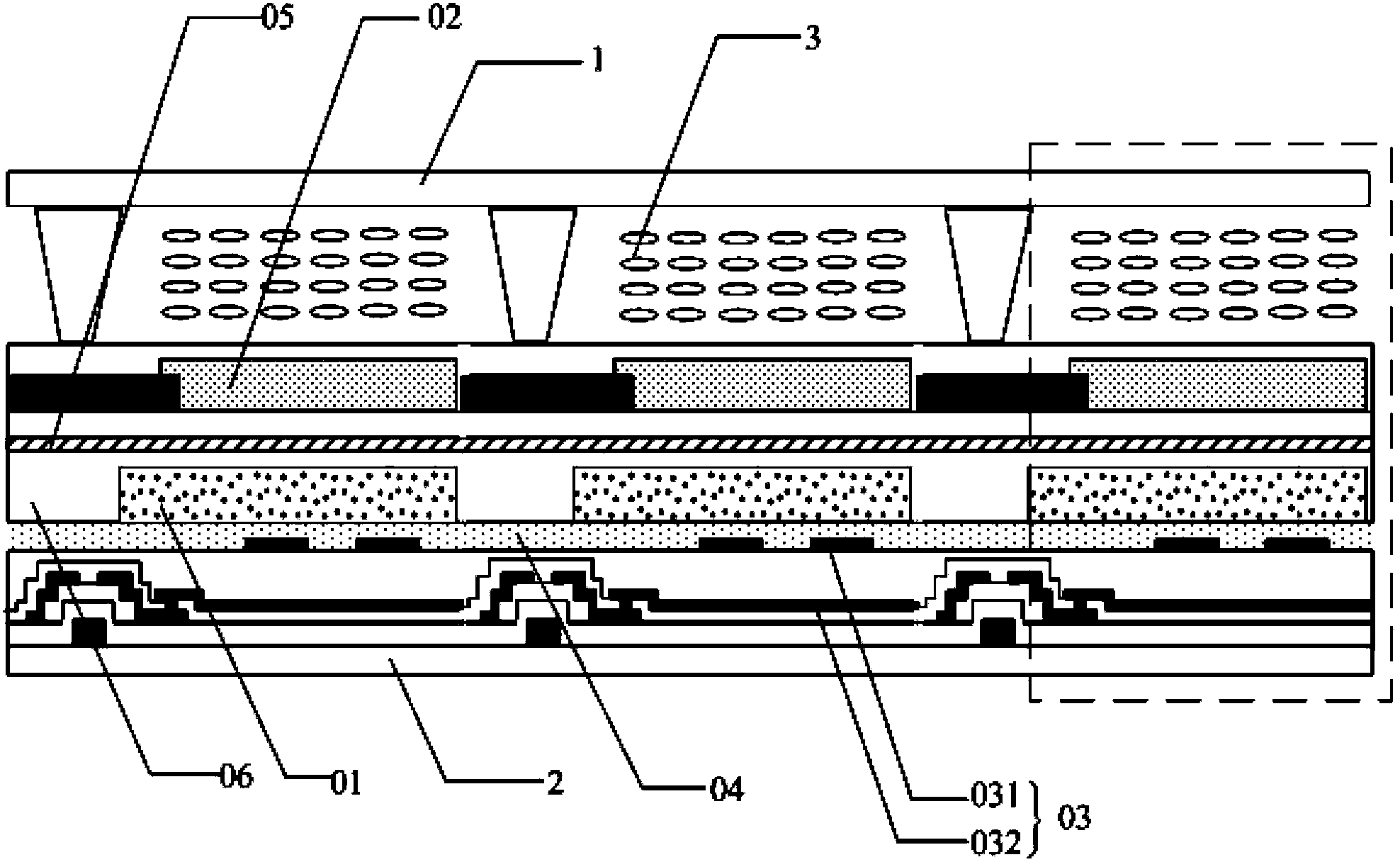
[0063] The color filter 02 in the liquid crystal display is arranged on the array substrate 2, and the manufacturing process of the array substrate 2 includes the following steps in addition to steps (1) to (13) in Example 1:

[0064] (14) Forming a black matrix 14 on the resin layer 13, such as Figure 4a shown;

[0065] (15) Form the color filter 02 on the resin layer 13, such as Figure 4b shown;

[0066] (16) Form a protective layer 15 on the black matrix 14 and the color filter 02, such as Figure 4c shown.

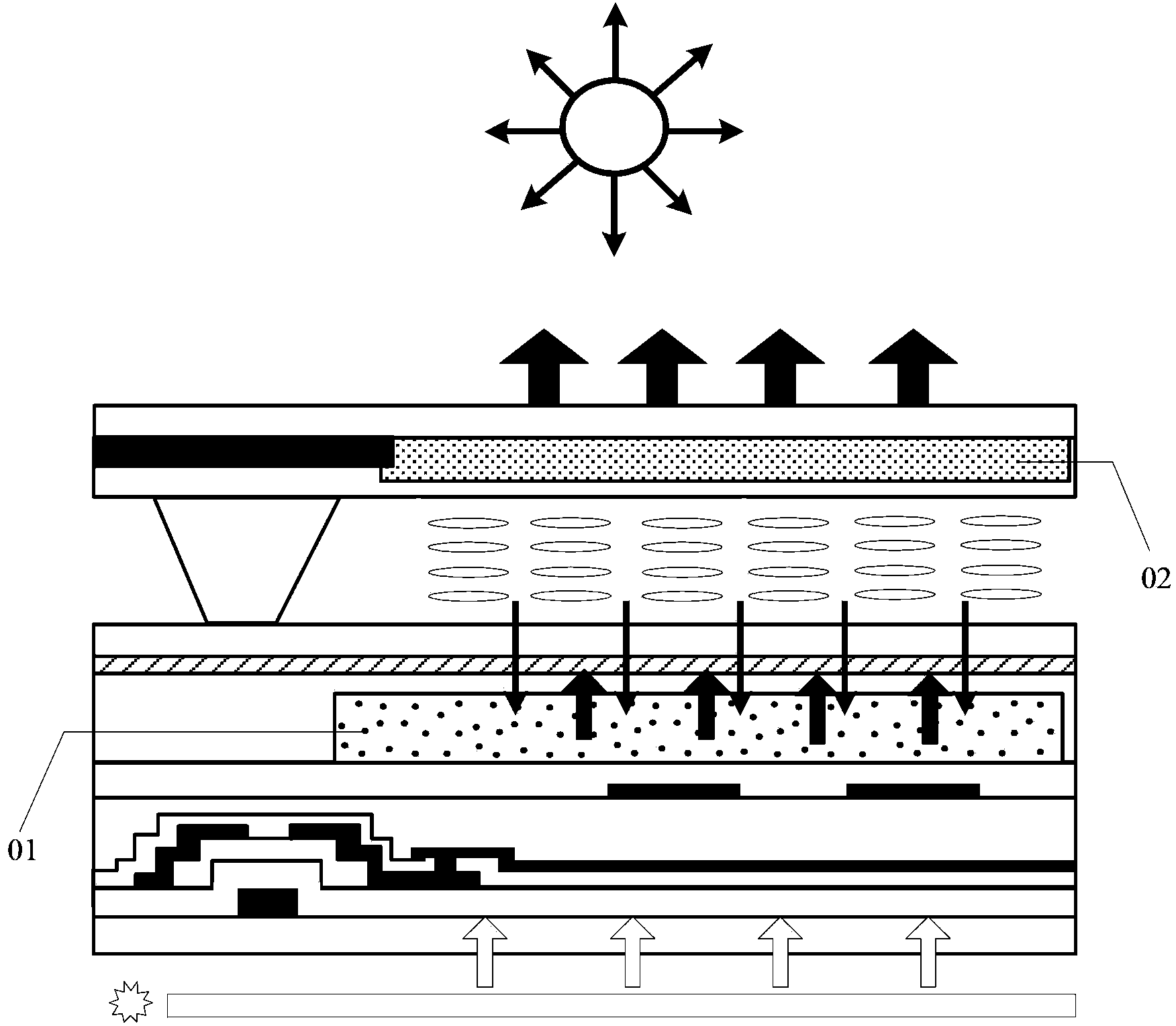
[0067] Based on the same inventive concept, an embodiment of the present invention also provides a display device, including the above-mentioned liquid crystal display provided by the embodiment of the present invention. Since the problem-solving principle of the device is similar to that of the aforementioned liquid crystal display, the implementation of the device Reference can be made to its implementation, and repeated descriptions will not be repeated here. ...


PUM

PropertyMeasurementUnit
particle diameteraaaaaaaaaa

Abstract

The invention discloses an LCD screen and a display device, wherein a plurality of pixel units are arranged in the LCD screen, and each pixel unit is provided with a plurality of sub-pixel units displaying different colors; a quantum dot layer through which back light can penetrate is arranged in a position of an array substrate corresponding to a sub-pixel unit with at least one color of each pixel unit; the quantum dot layer emits light containing at least the color of corresponding sub-pixel unit after excited by ultraviolet light in sunlight; and a color filter is located between the quantum dot layer and an opposite substrate. When the LCD is used for displaying outdoors, the ultraviolet light in the sunlight irradiates the quantum dot layer, and the quantum dot layer emits light after excited by the ultraviolet light, so that light penetrating through the color filter is the sum of the back light and the light emitted by the quantum dot layer after the quantum dot layer is excited, the display luminance of the LCD screen is enhanced, and the viewability of the LCD outdoors is improved.

Description

technical field [0001] The invention relates to the technical field of liquid crystal display, in particular to a liquid crystal display screen and a display device. Background technique [0002] Quantum Dots (QDs), also known as nanocrystals, are nanoparticles composed of II-VI or III-V elements. The particle size of quantum dots is generally between 1 and 20 nm. Since electrons and holes are quantum-confined, the continuous energy band structure becomes a discrete energy level structure, which can emit fluorescence after being excited. [0003] The emission spectrum of quantum dots can be controlled by changing the size of quantum dots. By changing the size of the quantum dot and its chemical composition, its emission spectrum can cover the entire visible light region. Taking CdTe quantum dots as an example, when its particle size grows from 2.5nm to 4.0nm, their emission wavelength can be red-shifted from 510nm to 660nm. [0004] At present, quantum dots can be used as...

Claims


Application Information

Patent Timeline
Patent Type & Authority Applications(China)
IPC IPC(8): G02F1/1335G02F1/136
CPCB82Y30/00C09K11/565G02B5/201G02F1/133514G02F1/133617G02F1/1362G02F2201/086G02F2202/108G02F2202/36G02F2203/01G02F1/133357G02F1/133565G02F1/133614G02F1/133638G02F1/136222B82Y20/00G02F1/13363G02F1/134336G02F1/1368
Inventor 郭仁炜董学郭建
Owner BEIJING BOE OPTOELECTRONCIS TECH CO LTD
Why Eureka
Try Eureka