Supercharge Your Innovation With Domain-Expert AI Agents!

Method of inspecting printed circuit boards of semiconductor packages

A technology for printed circuit boards and semiconductors, which is applied in the field of PCB inspection of semiconductor packages, and can solve the problems of delay in manufacturing process and increase in PCB inspection time.

Active Publication Date: 2016-04-20
HANMI SEMICON CO LTD
View PDF5 Cites 0 Cited by
  • Summary
  • Abstract
  • Description
  • Claims
  • Application Information

AI Technical Summary

Problems solved by technology

[0017] Therefore, the visual system photographs the marking of each mounting area in a static state, thereby increasing the inspection time of the PCB and delaying the entire manufacturing process

Method used


Image

  • Method of inspecting printed circuit boards of semiconductor packages
  • Method of inspecting printed circuit boards of semiconductor packages
  • Method of inspecting printed circuit boards of semiconductor packages

Examples


Embodiment Construction

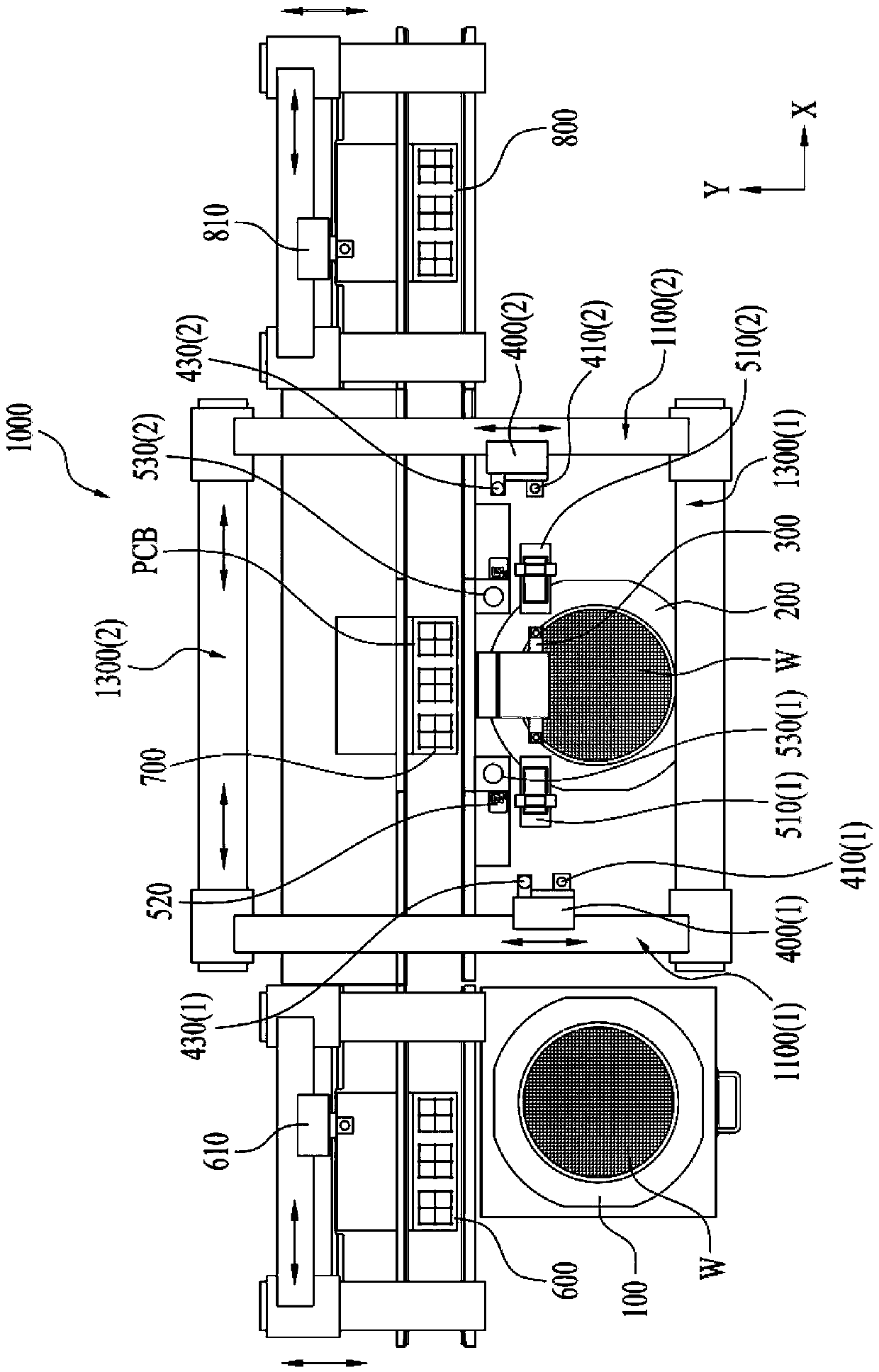
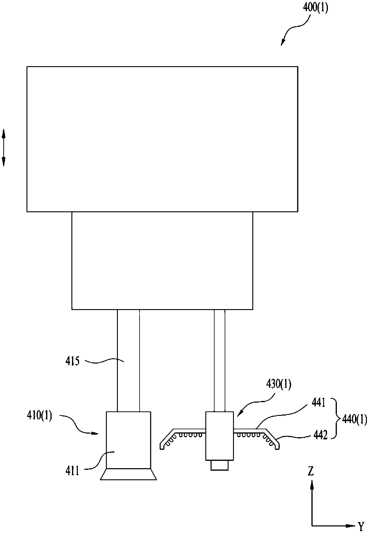
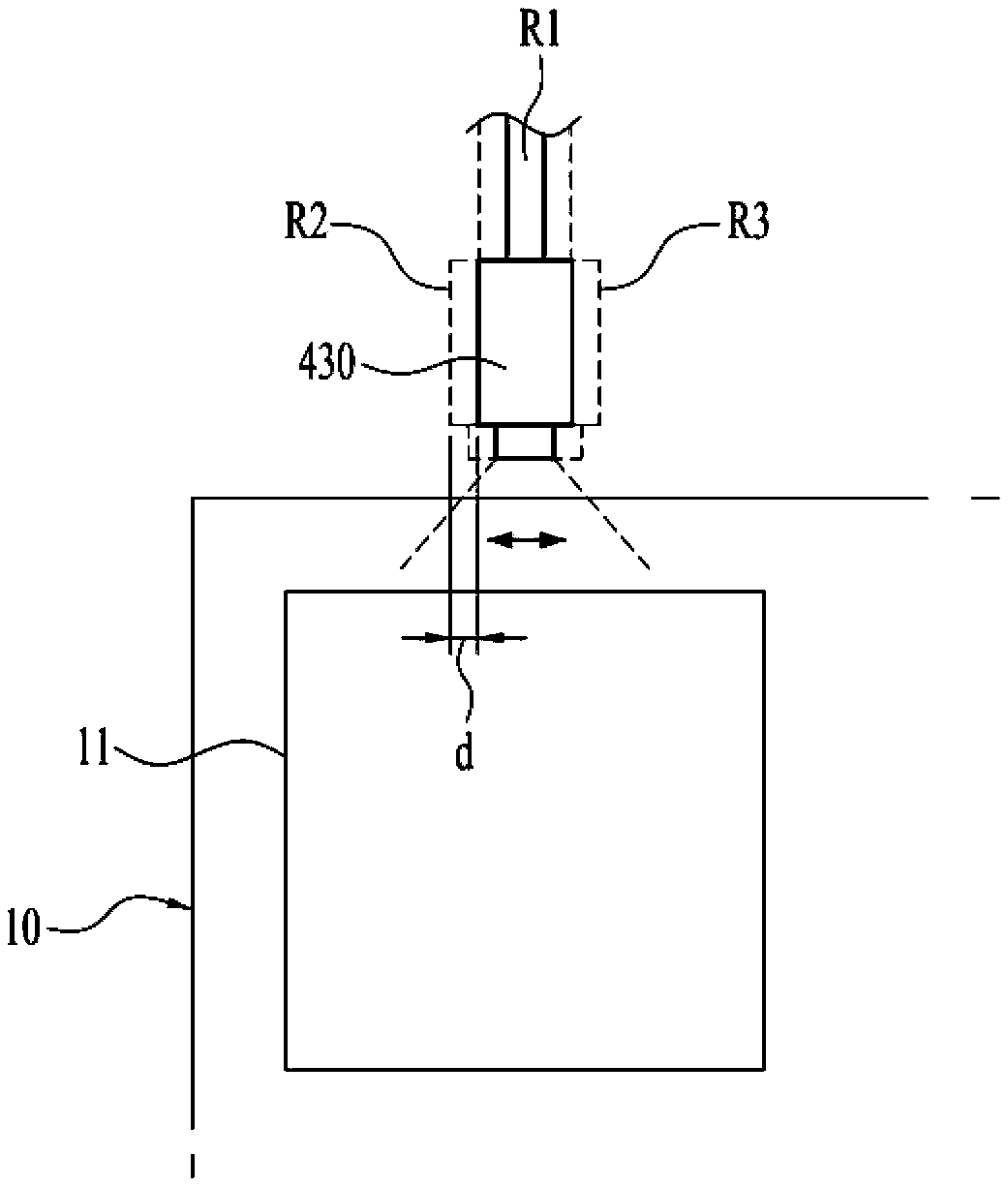
[0058] Reference will now be made in detail to the preferred embodiments of the invention, examples of which are illustrated in the accompanying drawings. Wherever possible, the same reference numbers will be used throughout the drawings to refer to the same or like parts.

[0059] Hereinafter, a method of inspecting a printed circuit board (PCB) of a semiconductor package according to an embodiment of the present invention will be described in detail with reference to the accompanying drawings. The drawings are for illustration only and are provided to fully describe embodiments of the invention. Accordingly, the drawings should not be construed as limiting the scope of the invention.

[0060] Furthermore, like reference numerals designate like or corresponding elements throughout the drawings, and a detailed description of these elements may be provided only once. In the drawings, the size and shape of elements may be exaggerated or reduced for convenience of illustration....


PUM


Abstract

The invention provides a method of inspecting a printed circuit board for a semiconductor package, wherein the method may increase accuracy when photographing patterns of mounting regions of the PCB, may secure sufficient total inspection time without reducing unit per hour (UPH), and may rapidly inspect defects of the mounting regions of the PCB. The method can be executed by a coupling device, which comprises: a wafer supply unit; a coupling bench; a coupling extractor which conveys a plurality of chips to the coupling bench; and a first visible system, for photographing installation areas permitting chip installation thereof respectively for the PCB. The method comprises: preparing the PCB with the plurality of installation areas permitting chip installation thereon respectively; executing multiple image photograph for each installation area of the PCB arranged on the coupling bench by the first visible system, so as to obtain multiple position values of each installation area of the PCB; and determining final position values of each installation area of the PCB based on the multiple position values.

Description

[0001] This application claims the benefit of Korean Patent Application No. 10-2012-0048631 filed on May 8, 2012 and Korean Patent Application No. 10-2012-0063195 filed on June 13, 2012, which are incorporated herein by reference For reference, as fully set forth here. technical field [0002] The present invention relates to a method of inspecting a printed circuit board (PCB) of a semiconductor package, and more particularly, to a method that can improve accuracy when photographing a pattern of a PCB mounting area, sufficiently secure the total inspection time without reducing yield per hour (UPH), and A method of inspecting a PCB of a semiconductor package for quickly inspecting defects in a PCB mounting area. Background technique [0003] In general, a process of attaching a semiconductor chip to a PCB having a plurality of mounting regions in which the semiconductor chip is fixed needs to be performed with high precision. [0004] In addition, the semiconductor chip an...

Claims


Application Information

Patent Timeline
Patent Type & Authority Patents(China)
IPC IPC(8): H01L21/66H01L21/50
CPCH01L22/12H01L22/24H01L24/83H01L2224/83908
Inventor 郑显权池升龙李贞均
Owner HANMI SEMICON CO LTD
Features
  • R&D
  • Intellectual Property
  • Life Sciences
  • Materials
  • Tech Scout
  • Unparalleled Data Quality
  • Higher Quality Content
  • 60% Fewer Hallucinations
Learn More