A storage material and its application in non-volatile charge-trap storage devices

A charge trapping, non-volatile technology, applied in the field of microelectronic materials, which can solve problems such as difficulty in meeting the requirements of memory miniaturization, polysilicon floating gate charge loss, leakage current, etc.

Inactive Publication Date: 2016-05-11
NANJING UNIV
View PDF2 Cites 0 Cited by
  • Summary
  • Abstract
  • Description
  • Claims
  • Application Information

AI Technical Summary

Problems solved by technology

With the gradual reduction of the feature size of semiconductor devices and the continuous improvement of integration, floating gate non-volatile memory devices face serious leakage current problems, and it is difficult to meet the miniaturization requirements of memory
As the size of the tunneling layer continues to decrease in floating-gate memory devices, a single defect can lead to the loss of all charge stored in the polysilicon floating gate

Method used


Image

  • A storage material and its application in non-volatile charge-trap storage devices
  • A storage material and its application in non-volatile charge-trap storage devices
  • A storage material and its application in non-volatile charge-trap storage devices

Examples


Embodiment 1

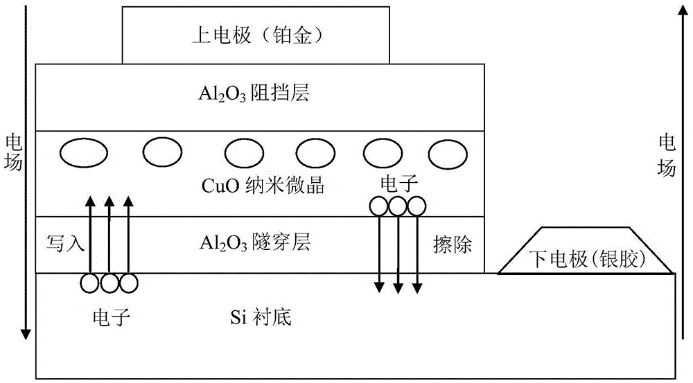
[0024] a) Use P-type Si as the substrate, and after cleaning, use ALD (vacuum atomic layer deposition or vacuum coating) technology to grow Al with a thickness of about 2-10nm on the surface 2 O 3 As a tunneling layer;

[0025] b) Using magnetron sputtering technology to grow uniform composition (CuO) on the tunnel layer X (Al 2 O 3 ) 1-x Thin film as storage layer;

[0026] c) Use ALD to grow another layer of Al about 15nm thick on the storage layer 2 O 3 As a barrier

[0027] d) Anneal the sample prepared above at a temperature lower than the melting point of CuO to make CuO nanocrystals precipitate out of the storage layer and be Al 2 O 3 Surrounded by amorphous matrix phase, the CuO nanocrystal is used as a storage medium; annealing is performed in a rapid annealing furnace, the annealing time is 20-60S, the annealing atmosphere is a nitrogen atmosphere, and the annealing temperature is 200±15°C; e) after annealing Magnetron sputtering was used to grow platinum with a thickness o...

Embodiment 2

[0028] Embodiment 2: Based on the Si substrate, the preparation process of the CuO nanocrystalline-based nonvolatile charge trapping memory device is specifically as follows:

[0029] a) Put the Si substrate in an appropriate amount of acetone, ultrasonically clean for 10 minutes, then use deionized water for ultrasonic cleaning for 10 minutes to remove the remaining substances on the substrate surface, and then put the substrate into the diluted hydrofluoric acid solution Soak in the medium for about 30 seconds to remove the surface oxides, and then use deionized water for ultrasonic cleaning for 5 minutes to wash off the residual hydrofluoric acid, dry it with high-purity nitrogen, and put it into the atomic layer chemical vapor deposition chamber to deposit the film.

[0030] b) Al(CH 3 ) 3 As the metal source, ozone is the oxygen source. Al deposited with a thickness of 3nm 2 O 3 As a tunneling layer.

[0031] c) Then put the sample into the magnetron sputtering growth chamber, ...


PUM


Abstract

Provided are charge storage materials in a nonvolatile charge trapping type memory device. The storage materials are mixed oxide materials, namely, (CuO) x (Al2O3) 1-x mixed oxide materials, and the value of x is 0.1-0.8. The invention further discloses the application of the charge storage materials in the nonvolatile charge trapping type memory device. According to the structure of the nonvolatile charge trapping type memory device, a tunneling layer Al2O3 / a storage layer film (CuO) X (Al2O3) 1-x / a barrier layer Al203 is grown on a semiconductor substrate in sequence, (CuO) x (Al2O3) 1-x is a storage layer, and CuO nanocrystalline obtained from the charge storage materials (CuO) X (Al2O3) 1-x through annealing has the function of storing dielectric materials.

Description

Technical field [0001] The invention belongs to the field of microelectronic materials, and relates to a new type of storage material and its application in a non-volatile charge trapping storage device. Background technique [0002] Since the birth of non-volatile semiconductor memory, floating gate memory has been a mainstream product in the memory market. As the feature size of semiconductor devices gradually shrinks and the integration level continues to increase, floating gate non-volatile memory devices face serious leakage current problems, and it is difficult to meet the miniaturization requirements of memories. As the size of the tunneling layer in floating gate memory devices continues to decrease, one defect will cause all the charges stored in the polysilicon floating gate to be lost. Therefore, finding a non-volatile memory with high storage density, fast programming, low cost, and low energy consumption has become a hot spot in the current memory research field. P...

Claims


Application Information

Patent Timeline
Patent Type & Authority Patents(China)
IPC IPC(8): H01L29/51H01L27/115H01L27/11568
Inventor 卢伟徐波夏奕东殷江刘治国
Owner NANJING UNIV
Why Eureka
Try Eureka