
Recovery circuit and recovery method for positive bias temperature instability

A technology of positive bias temperature and instability, applied in logic circuits, electrical components, pulse technology, etc., can solve the problems of NMOS transistors, such as the influence of positive bias temperature instability, threshold voltage shift, etc., and achieve good PBTI characteristics The effect of recovery effect

Active Publication Date: 2016-01-06
SEMICON MFG INT (SHANGHAI) CORP
View PDF3 Cites 0 Cited by
  • Summary
  • Abstract
  • Description
  • Claims
  • Application Information

AI Technical Summary

Problems solved by technology

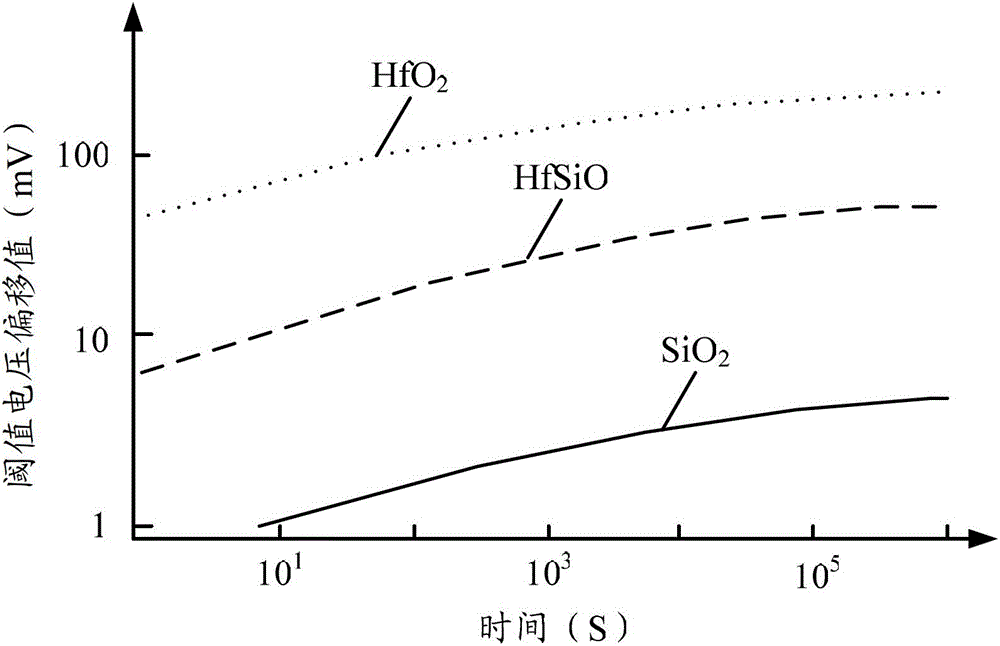
It can be clearly seen from the figure that the SiO 2 As the material of the gate dielectric layer, it is not easy to cause the threshold voltage to shift, and the use of HfO 2 High-K dielectric materials such as HfSiO are more likely to cause threshold voltage shifts as gate dielectric materials, and NMOS transistors using high-K / metal gate stack structures are more susceptible to positive bias temperature instability

Method used


Image

  • Recovery circuit and recovery method for positive bias temperature instability
  • Recovery circuit and recovery method for positive bias temperature instability
  • Recovery circuit and recovery method for positive bias temperature instability

Examples


Embodiment Construction

[0035]The inventors have found through research that the temperature instability of the positive bias voltage has an obvious recovery effect. Since the channel region of the NMOS transistor needs to be applied with a positive bias gate voltage, and the high-K / metal gate stack structure is easy to capture electrons in the high-K gate dielectric layer and Si, it is easy to make the high-K metal gate stack structure The threshold voltage of the NMOS transistor is shifted, so that the NMOS transistor has a PBTI characteristic. When the gate voltage becomes smaller, that is, when the absolute value of the gate voltage becomes smaller or becomes a negatively biased gate voltage, the NMOS transistor can return to a more normal state, and when the absolute value of the gate voltage The NMOS transistor recovers to a more normal state faster and better when the value is changed to a negatively biased gate voltage. However, since the operating voltage value applied to the gate in existi...


PUM


Abstract

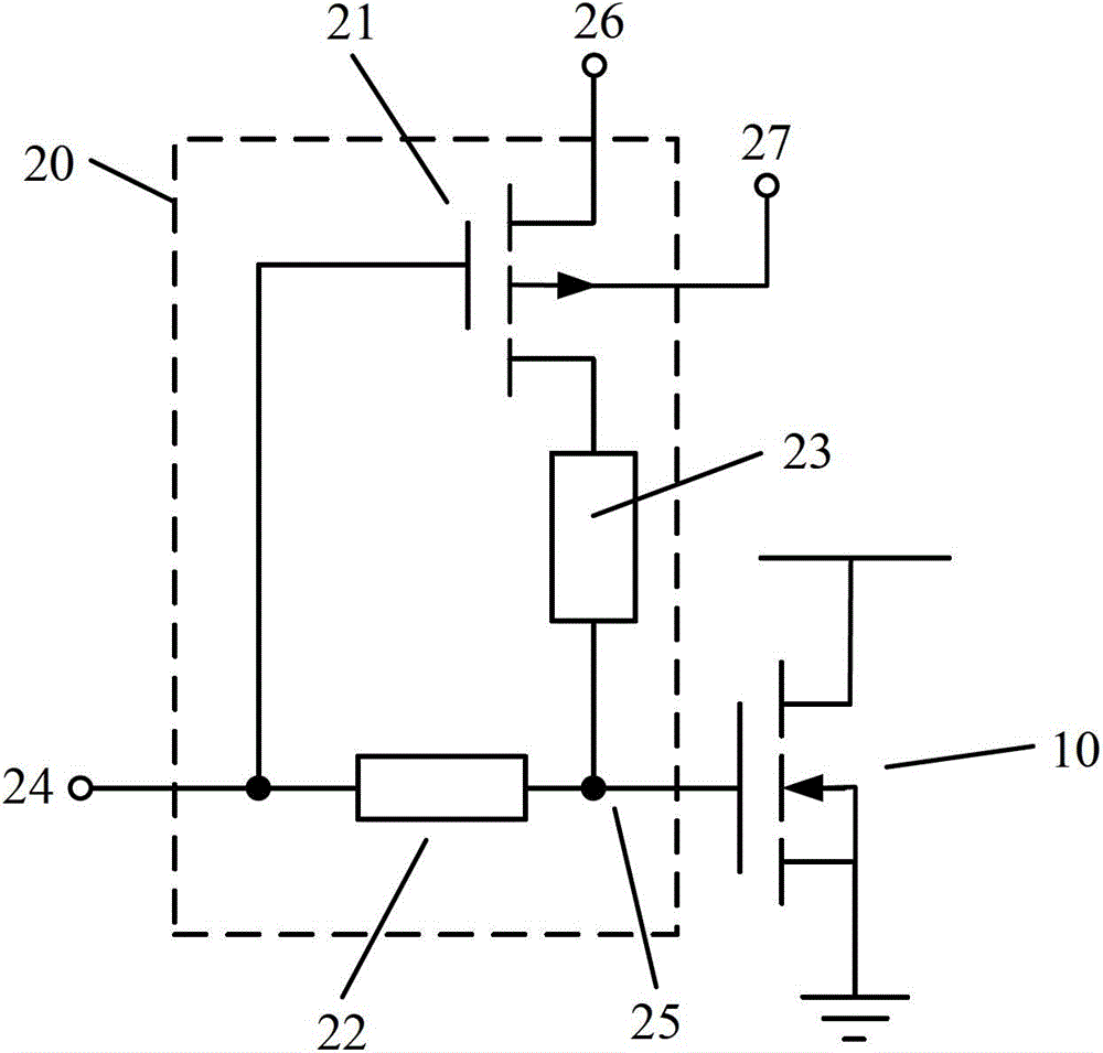
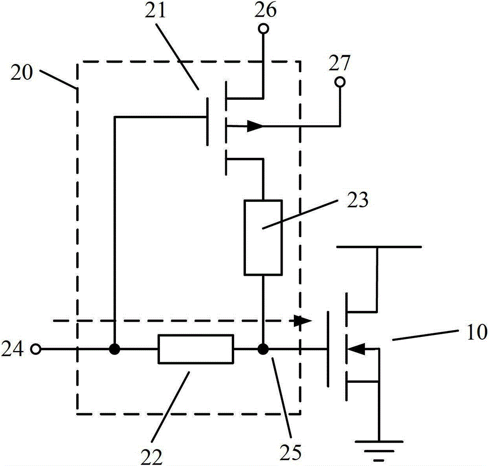
Provided are a restoring circuit and restoring method against positive bias temperature instability. The restoring circuit comprises a to-be-restored N-channel metal oxide semiconductor (NMOS) transistor and a restoring unit. A grid electrode of the to-be-restored NMOS transistor is connected with the restoring unit. According to the restoring unit, a grid electrode of a switch transistor is connected with a signal input end, a drain electrode of the switch transistor is connected with a first voltage end, the first voltage end provides a negative first working voltage, a substrate of the switch transistor is connected with a second voltage end, a source electrode of the switch transistor is connected with one end of a second resistor, the other end of the second resistor is connected with a signal output end, one end of a first resistor is connected with a signal input end, and the other end of the first resistor is connected with the signal output end. Due to the fact that the voltage of the first voltage end is negative, by adjusting resistance values of the first resistor and the second resistor, grid electrode voltage applied to the to-be-restored NMOS transistor can be negative pressure, and good positive bias temperature instability (PBTI) characteristic restoration effect can be achieved.

Description

technical field [0001] The invention relates to the field of semiconductors, in particular to a recovery circuit and recovery method for positive bias temperature instability. Background technique [0002] As the integration level of semiconductor integrated circuits becomes higher and higher, the requirements for the performance of transistors are also increased, and therefore, the requirements for the reliability of transistors are also increased. In the CMOS process, when evaluating the reliability of the PMOS transistor, the negative bias temperature instability (NegativeBiasTemperatureInstability, NBTI) is a main evaluation factor. Negative bias temperature instability means that under the action of negative bias gate voltage and high temperature of the PMOS transistor, the hydrogen-silicon bond at the interface between the gate oxide layer of the PMOS transistor and the substrate is broken, forming interface defect charges, thereby A phenomenon that causes the thresho...

Claims


Application Information

Patent Timeline
Patent Type & Authority Patents(China)
IPC IPC(8): H03K19/094
Inventor 冯军宏甘正浩
Owner SEMICON MFG INT (SHANGHAI) CORP
Learn More