Correction method of optical proximity correction model

A technology of optical proximity correction and proximity correction, which is applied in the direction of optics, originals for photomechanical processing, and photoplate-making process of pattern surface, etc., can solve the problem of long time-consuming optical proximity correction model correction, and reduce the cost Time, reduce the amount of calculation, the effect of short time consumption

Active Publication Date: 2013-12-25
SEMICON MFG INT (SHANGHAI) CORP
View PDF8 Cites 13 Cited by
  • Summary
  • Abstract
  • Description
  • Claims
  • Application Information

AI Technical Summary

Problems solved by technology

[0008] The problem solved by the invention is that it takes a long time to correct the optical proximity correction model in the prior art

Method used


Image

  • Correction method of optical proximity correction model
  • Correction method of optical proximity correction model

Examples


Embodiment Construction

[0063] In order to make the above objects, features and advantages of the present invention more comprehensible, specific implementations of the present invention will be described in detail below in conjunction with the accompanying drawings.

[0064] In the following description, specific details are set forth in order to provide a thorough understanding of the present invention. However, the present invention can be implemented in many other ways than those described here, and those skilled in the art can make similar extensions without departing from the connotation of the present invention. Accordingly, the present invention is not limited to the specific embodiments disclosed below.

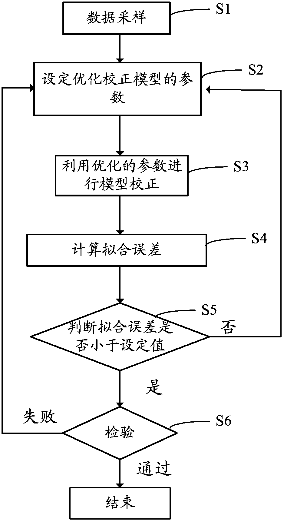
[0065] figure 2 It is a schematic flowchart of a method for correcting an optical proximity correction model according to a specific embodiment of the present invention, refer to figure 2 , the method for correcting the optical proximity correction model in a specific embodiment of the ...


PUM


Abstract

A correction method of an optical proximity correction model comprises providing a semiconductor substrate with a figure; performing data sampling of the figure to obtain sampling data; dividing the sampling data into a first group of data and a second group of data; correcting the optical proximity correction model to be corrected by use of the first group of data to obtain a corrected optical proximity correction model; using the corrected optical proximity correction model to obtain an analog figure, performing data sampling of the analog figure to obtain analog data, with an error between the analog data corresponding to the first group of data and the first group of data being less than a predetermined value; judging if an error between the analog data corresponding to the second group of data and the second group of data being less than a predetermined value; if the judgment result is yes, using the corrected optical proximity correction model as a well corrected optical proximity correction model; and if the judgment result is no, correcting again the optical proximity correction model to be corrected. Through use of the technical scheme, relatively little time is needed for correction of the optical proximity correction model to be corrected.

Description

technical field [0001] The invention relates to the technical field of semiconductors, in particular to a method for correcting an optical proximity correction model. Background technique [0002] In the semiconductor manufacturing process, the photolithography process is one of the most important process steps in the production of integrated circuits. With the development of semiconductor manufacturing technology, the feature size is getting smaller and smaller, and the requirements for resolution in the photolithography process are getting higher and higher. Lithography resolution refers to the minimum feature size (critical dimension, CD) that can be exposed on the surface of a silicon wafer by a lithography machine, and is one of the important performance indicators in lithography technology. [0003] However, with the development of semiconductor technology, the feature size of semiconductor devices is getting smaller and smaller. When the feature size is close to or e...

Claims


Application Information

Patent Timeline
Patent Type & Authority Applications(China)
IPC IPC(8): G03F1/36
Inventor 黄宜斌
Owner SEMICON MFG INT (SHANGHAI) CORP
Why Eureka
Try Eureka