Touch screen, method for manufacturing same and display device
A technology for display devices and touch screens, which is applied in the fields of instruments, calculations, electrical digital data processing, etc., and can solve problems such as high resistivity, poor touch effect, and large signal delay
- Summary
- Abstract
- Description
- Claims
- Application Information
AI Technical Summary
Problems solved by technology
Method used
Image
Examples
Embodiment 1
[0093] Embodiment 1: Based on a one-and-a-half-layer touch screen.
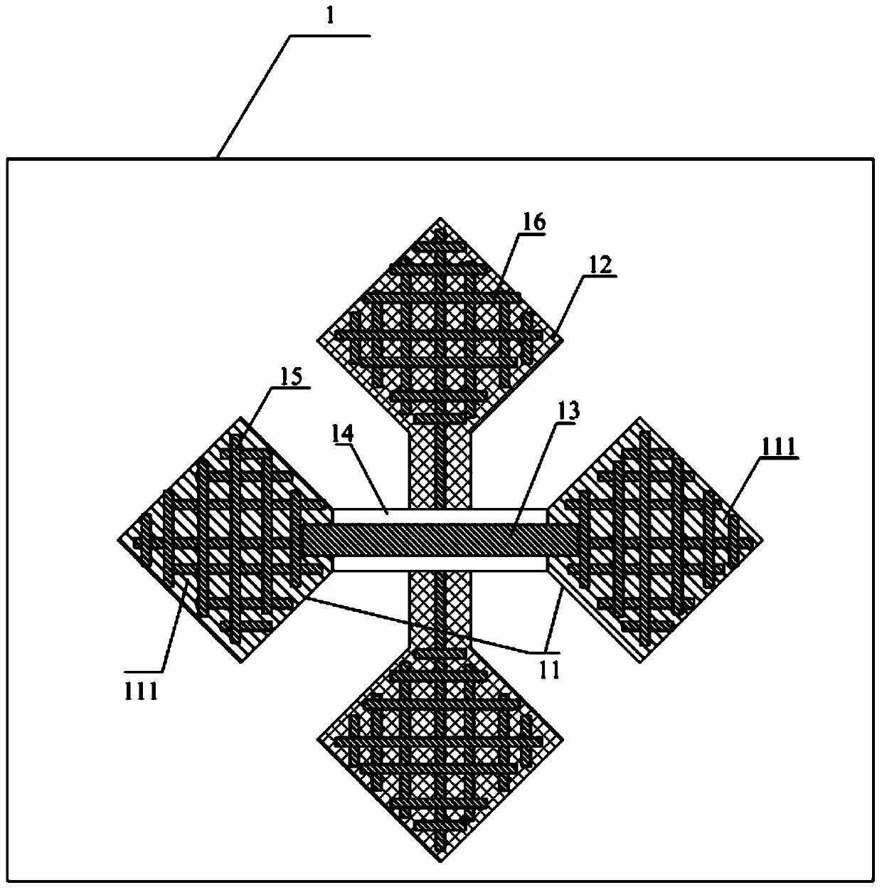
[0094] see figure 1 , which is a schematic top view of the touch screen provided in Embodiment 1 of the present invention, including:
[0095] Substrate 1;
[0096] A plurality of first transparent electrodes 11 arranged along the first direction on the substrate 1;
[0097] A plurality of second transparent electrodes 12 ( figure 2 Only one first transparent electrode 11 and one second transparent electrode 12 are shown in );
[0098] The first transparent electrode 11 is disconnected into a plurality of first transparent sub-electrodes 111 in the intersection area, and two adjacent first transparent sub-electrodes 111 are electrically connected through the conductive sheet 13; The electrodes 12 are insulated by an insulating layer 14 .
[0099] Wherein, the conductive sheet may be a metal lead, a transparent electrode lead or the like.
[0100] The first direction and the second direction are perpend...
Embodiment 2
[0126] Embodiment 2: Based on a double-layer touch screen.
[0127] see Figure 6 , the touch screen provided by Embodiment 2 of the present invention includes:
[0128] Substrate 1;
[0129] A plurality of first transparent electrodes 11 arranged along the first direction on the substrate 1;
[0130] A plurality of second transparent electrodes 12 arranged along the second direction on the substrate 1 ( Figure 6 Only one first transparent electrode 11 and one second transparent electrode 12 are shown in );
[0131] The first transparent electrode 11 is insulated from the second transparent electrode 12 by an insulating layer 14 at least in the intersection area;
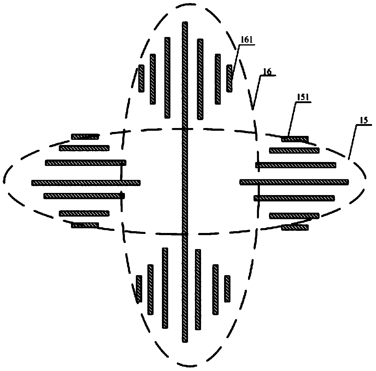
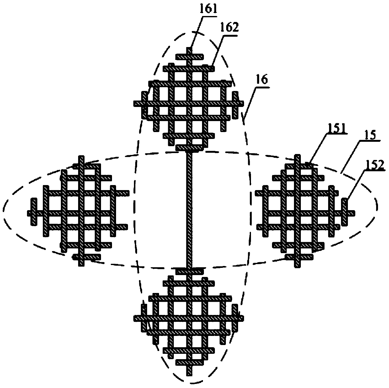
[0132] Wherein, at least one side of the first transparent electrode 11 is provided with a first conductive layer 15, and the first conductive layer 15 is located in the area where the first transparent electrode 11 is located; and / or at least one side of the second transparent electrode 12 is provided with a s...
Embodiment 3
[0136] Embodiment 3: Based on a single-layer touch screen.
[0137] see Figure 7 , the touch screen provided by embodiment three includes:
[0138] Substrate 1;
[0139] A plurality of first transparent electrodes 11 arranged along the first direction on the substrate 1;
[0140] A plurality of second transparent electrodes 12 arranged along the first direction on the substrate 1;
[0141] Two adjacent first transparent electrodes 11 and second transparent electrodes 12 are coupled, and there is no crossing, no crossing, and no intersection between the two, that is, the first transparent electrodes 11 and the second transparent electrodes 12 are insulated, and on the substrate 1 There is no overlap in the projection; at least one side of the first transparent electrode 11 is provided with a first conductive layer 15, and the first conductive layer 15 is located in the area where the first transparent electrode 11 is located; and / or at least one side of the second transpare...
PUM
 Abstract
Description
Claims
Application Information


