Copper foil for printed wiring board, process for preparing the same, and printed wiring board using the copper foil
A technology of printed circuit boards and copper foils, which is applied in the fields of printed circuit manufacturing, printed circuits, printed circuit parts, etc., can solve the problems of poor adhesion, difficulty in forming copper wiring patterns, and longer etching time, etc., to achieve adhesion Good contact effect
- Summary
- Abstract
- Description
- Claims
- Application Information
AI Technical Summary
Problems solved by technology
Method used
Image

Examples
Embodiment 1
[0080] In Example 1, first, an electrolytic copper foil having a thickness of 12 μm and a size of 150 mm×150 mm was prepared. Next, the glossy surface of the prepared electrodeposited copper foil is etched. The composition and etching conditions of the etching liquid composition are as follows. Here, the glossy surface refers to the surface on the side contacting the roll-shaped cathode among both surfaces of the electrolytic copper foil.
[0081] ・Composition of etching liquid composition
[0082] Hydrogen peroxide: 0.5% by mass
[0083] Sulfuric acid: 2% by mass
[0084] 1H-tetrazole: 0.1% by mass
[0085] Chloride ion: 0.5ppm
[0086] · Etching conditions
[0087] Temperature of liquid composition for etching: 30°C
[0088] Injection pressure: 0.1MPa
[0089] Spray time: 1 minute
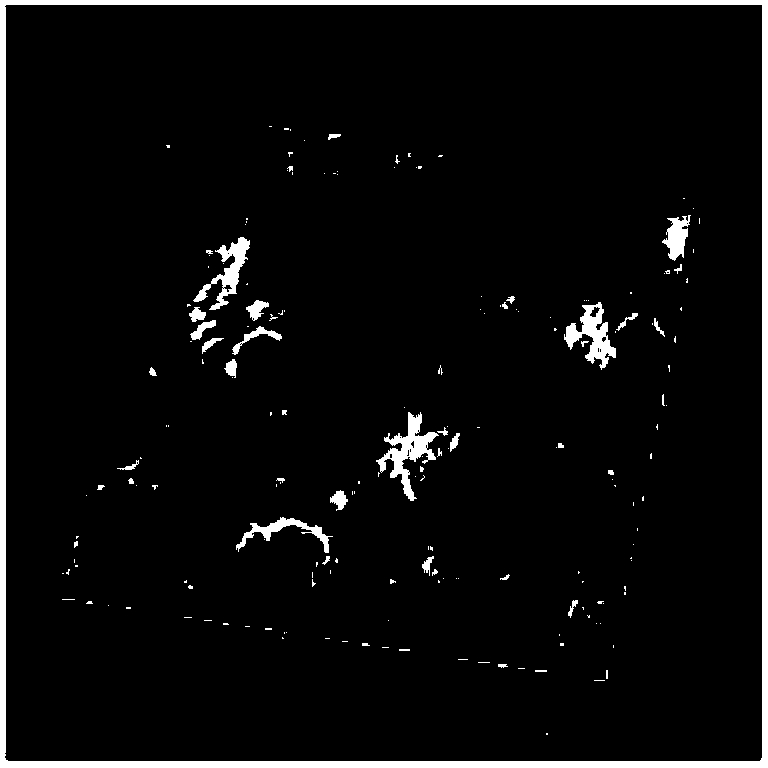
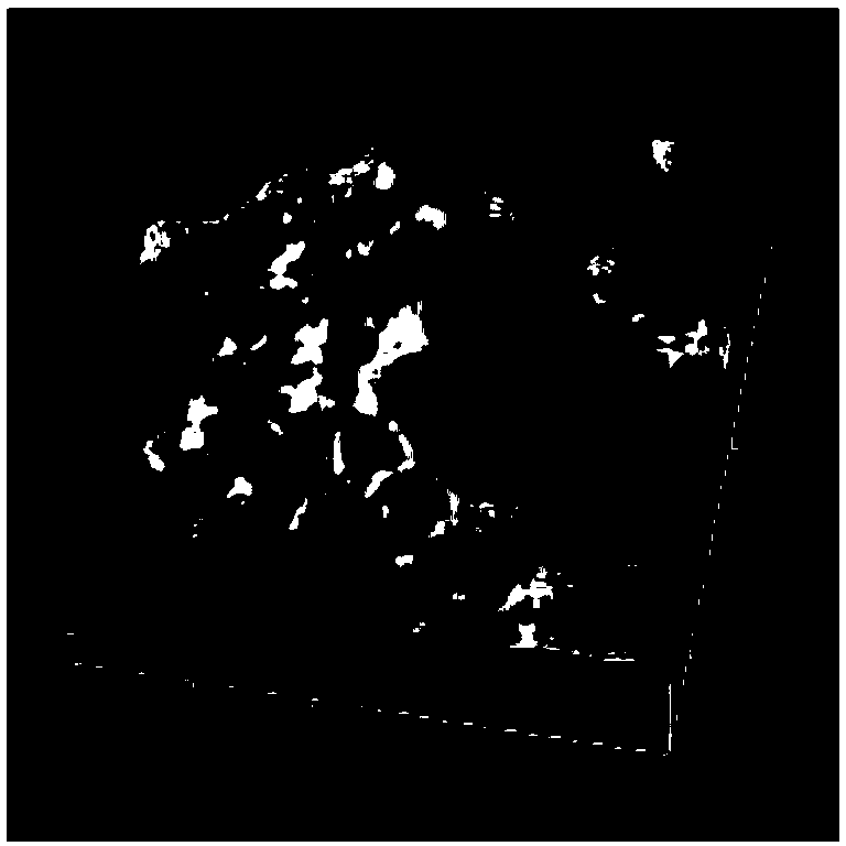
[0090] Next, the etched copper foil surface was observed with a scanning tunneling microscope at a magnification of 30000 times. figure 1 is a three-dimensional image of the copper foil...
Embodiment 2
[0129] In Example 2, the test similar to Example 1 was performed except having changed the liquid composition used for the etching process of the glossy surface of an electrolytic copper foil as follows.
[0130] ・Composition of etching liquid composition
[0131] Hydrogen peroxide: 0.5% by mass
[0132] Sulfuric acid: 2% by mass
[0133] 5-Methyltetrazole: 0.1% by mass
[0134] Chloride ion: 1ppm
[0135] The surface area in the region of 5 μm in length×5 μm in width of the copper foil surface after etching was measured. As a result, the surface area of the copper foil is 44.7 [μm 2 ].
[0136] The surface roughness (Rzjis: ten-point height of microscopic unevenness) of the copper foil after etching was measured. As a result, the surface roughness of the copper foil was 0.5 [μm].
[0137] The adhesion enhancement coefficient E was calculated based on the above general formula (1). As a result, the coefficient of adhesion enhancement E was 3.58. The calculation form...
Embodiment 3
[0143] In Example 3, the test similar to Example 1 was performed except having changed the liquid composition used for the etching process of the glossy surface of an electrolytic copper foil as follows.
[0144] ・Composition of etching liquid composition
[0145] Hydrogen peroxide: 1% by mass
[0146] Sulfuric acid: 2.5% by mass
[0147] 5-Methyltetrazole: 0.05% by mass
[0148] 1,5-Dimethyltetrazole: 0.05% by mass
[0149] Chloride ion: 1ppm
[0150] The surface area in the region of 5 μm in length×5 μm in width of the copper foil surface after etching was measured. As a result, the copper foil has a surface area of 38 [μm 2 ].
[0151] The surface roughness (Rzjis: ten-point height of microscopic unevenness) of the copper foil after etching was measured. As a result, the surface roughness of the copper foil was 0.25 [μm].
[0152] The adhesion enhancement coefficient E was calculated based on the above general formula (1). As a result, the coefficient of adhesion...
PUM
| Property | Measurement | Unit |
|---|---|---|
| Thickness | aaaaa | aaaaa |
| Surface roughness | aaaaa | aaaaa |
| Peel strength | aaaaa | aaaaa |
Abstract
Description
Claims
Application Information
 - R&D Engineer
- R&D Manager
- IP Professional
- Industry Leading Data Capabilities
- Powerful AI technology
- Patent DNA Extraction
Browse by: Latest US Patents, China's latest patents, Technical Efficacy Thesaurus, Application Domain, Technology Topic.
© 2024 PatSnap. All rights reserved.Legal|Privacy policy|Modern Slavery Act Transparency Statement|Sitemap