Resistive random access memory unit and manufacturing method thereof

A resistive memory and memory cell technology, applied in the field of microelectronics, can solve the problems affecting device stability, low rewritable times, slow read and write speed, etc., and achieve good light transmittance, prolong life, and reduce leakage current. Effect

Inactive Publication Date: 2014-01-08
UNIV OF SCI & TECH BEIJING
View PDF4 Cites 15 Cited by
  • Summary
  • Abstract
  • Description
  • Claims
  • Application Information

AI Technical Summary

Problems solved by technology

On the one hand, due to the high writing voltage of Flash memory, the reading and writing speed is slow (reading and writing / erasing time: 1ms / 0.1ms), and the erasable times are relatively low >10 5 Second-rate
On the other hand, the basic principle of Flash memory is to use floating gate charge storage technology to change the threshold characteristics of MOS transistors to realize data storage. Further reduction in size will lead to the corresponding gate insulating layer thickness being too small, resulting in the gradual emergence of electron tunneling effect and leakage current. increases sharply, thus affecting the stability of the device

Method used


Image

  • Resistive random access memory unit and manufacturing method thereof
  • Resistive random access memory unit and manufacturing method thereof
  • Resistive random access memory unit and manufacturing method thereof

Examples


Embodiment Construction

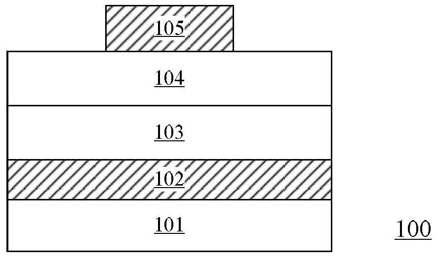
[0021] Hereinafter, the present invention will be described in more detail with reference to the accompanying drawings. For the sake of clarity, various parts in the drawings have not been drawn to scale.

[0022] It should be understood that when describing the structure of a device, when a layer or a region is referred to as being "on" or "over" another layer or another region, it may mean being directly on another layer or another region, or Other layers or regions are also included between it and another layer or another region. And, if the device is turned over, the layer, one region, will be "below" or "beneath" the other layer, another region. If it is to describe the situation directly on another layer or another area, the expression "directly on" or "on and adjacent to" will be used herein.

[0023] In the following, many specific details of the present invention are described, such as device structures, materials, dimensions, processing techniques and techniques, f...


PUM


Abstract

The invention discloses a resistive random access memory unit and a manufacturing method thereof. The resistive random access memory unit comprises a bottom electrode, a top electrode and a resistance change material laminated layer positioned between the bottom electrode and the top electrode, wherein the resistance change material laminated layer comprises at least two layers which are made of different resistance change materials and are directly contacted with each other. The resistive random access memory unit can be used for nonvolatile memories with high switch resistance ratio and high stability.

Description

technical field [0001] The invention belongs to the technical field of microelectronics, and in particular relates to a resistance variable memory unit and a manufacturing method thereof. Background technique [0002] Non-volatile memory has the characteristic of long-term preservation of internal storage data after power failure, making it widely used in various handheld terminal communication and multimedia equipment. At present, the mainstream non-volatile memory in the market is Flash memory. Flash memory has the advantages of simple structure, high storage density, electrical erasability, reprogrammability, low cost, high erasing speed and high reliability. There are obvious defects and problems in Flash memory. On the one hand, due to the high writing voltage of Flash memory, the reading and writing speed is slow (reading and writing / erasing time: 1ms / 0.1ms), and the erasable times are relatively low >10 5 Second-rate. On the other hand, the basic principle of Fl...

Claims


Application Information

Patent Timeline
Patent Type & Authority Applications(China)
IPC IPC(8): H01L45/00
Inventor 苗君张容姜勇徐晓光徐泽东
Owner UNIV OF SCI & TECH BEIJING
Why Eureka
Try Eureka