Contiguous printed circuit board and its cutting and transplanting process
A technology for printed circuit boards and process methods, applied in the field of electronics, can solve the problems of low connection accuracy and large connection gap, and achieve the effects of ensuring the connection accuracy, reducing the connection gap, and ensuring the splicing accuracy.
- Summary
- Abstract
- Description
- Claims
- Application Information
AI Technical Summary
Problems solved by technology
Method used
Image
Examples
Embodiment 1
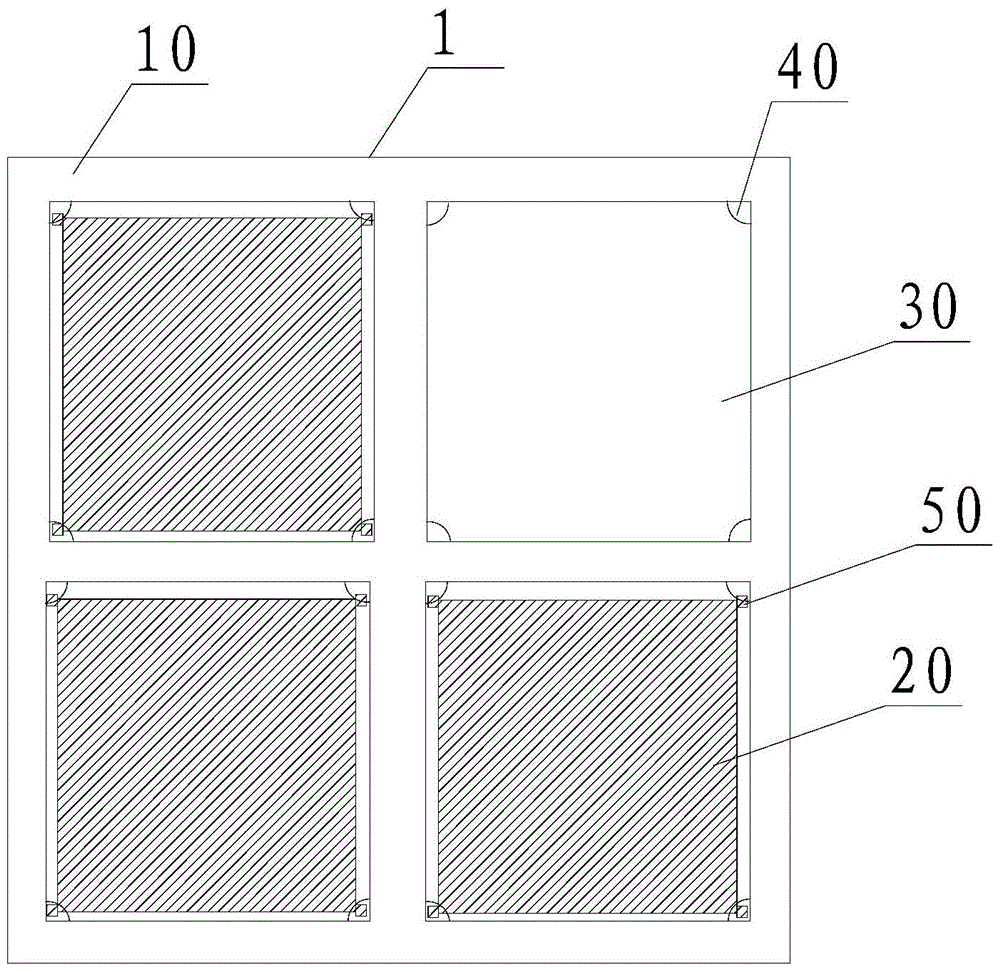
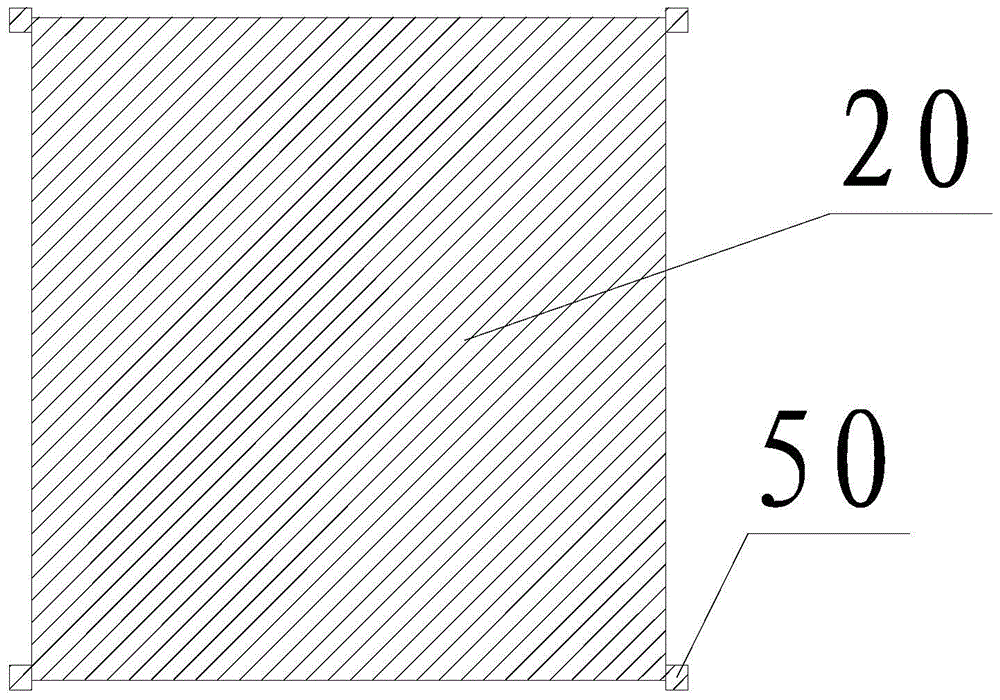
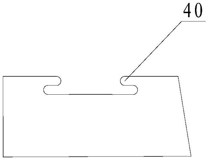
[0024] Such as figure 1 and figure 2 As shown, a contiguous printed circuit board 1 provided in Embodiment 1 of the present invention includes a substrate 10 and at least one single-piece board 20, and the substrate 10 is also provided with a mounting hole 30, and the mounting hole 30 is connected to the The shape of the single-piece plate 20 matches, and the edge of the installation hole 30 is uniformly provided with a plurality of outward flanged limiting parts 40;
[0025] The edge of the monolithic plate 20 is evenly provided with the same number of protruding parts 50 as the limit part, and the limit part 40 is matched with the protruding part 50; the limit part 40 on the substrate 10 is used for The protruding portion 50 on the single board 20 is buckled. The above-mentioned limiting parts with flanging are correspondingly distributed on both sides of the substrate. After being stuck, the protruding part can just be stuck in the cavity formed by the limiting parts on ...
Embodiment 2
[0042] Based on the same inventive concept, Embodiment 2 of the present invention also provides a cutting and transplanting process method for a contiguous printed circuit board. Since the problem-solving principle of this method is based on the structural principle of the aforementioned contiguous printed circuit board, repeated The place will not be repeated.
[0043] Such as Figure 5 As shown, Embodiment 2 of the present invention also provides a cutting and transplanting process for continuous printed circuit boards, including the following steps:
[0044] Step S100, using the second-dimensional optical measurement equipment to determine the offset direction of the optical points of a continuous printed circuit board;
[0045] Step S200, determine the position of the cutting positioning hole of another piece of continuous printed circuit board, perform the cutting operation, separate the cut substrate from the single board, and determine the deviation of the optical poin...
PUM
 Abstract
Description
Claims
Application Information


