A kind of multilayer pcb board manufacturing method and multilayer pcb board

A technology of PCB board and manufacturing method, which is applied in the field of electronic devices, can solve problems such as low production efficiency, expansion and contraction of inner layer boards, and increased difficulty of alignment, and achieve the effect of improving production efficiency

Active Publication Date: 2016-08-03
SHENNAN CIRCUITS
View PDF3 Cites 0 Cited by
  • Summary
  • Abstract
  • Description
  • Claims
  • Application Information

AI Technical Summary

Problems solved by technology

However, this traditional buried blind hole manufacturing process requires secondary lamination, and the production efficiency is low
In addition, the inner layer blind holes are processed before lamination. Since the processing of blind holes requires copper sinking and electroplating processes, it will inevitably lead to expansion and contraction of the inner layer board, which will lead to subsequent lamination and outer circuit processing. Matchup Difficulty Increased

Method used


Image

  • A kind of multilayer pcb board manufacturing method and multilayer pcb board
  • A kind of multilayer pcb board manufacturing method and multilayer pcb board
  • A kind of multilayer pcb board manufacturing method and multilayer pcb board

Examples


Embodiment 1

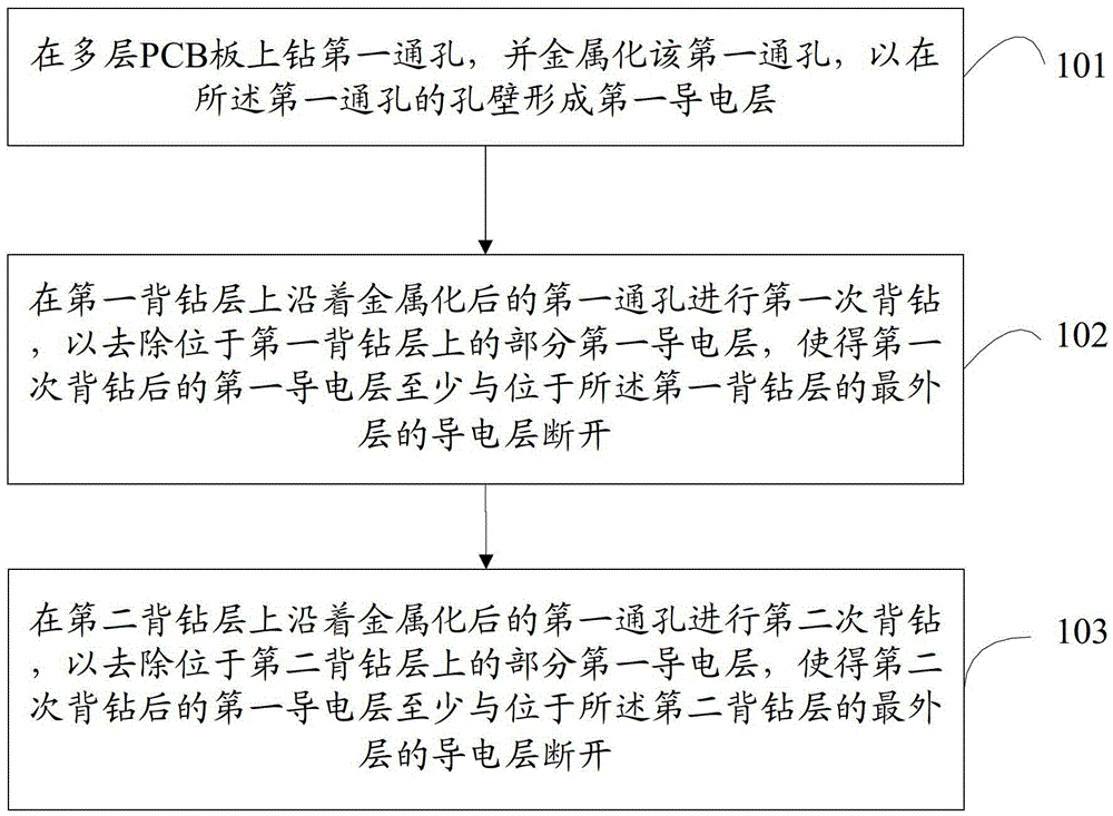
[0016] like figure 1 Shown, a kind of manufacturing method of multilayer PCB board comprises:

[0017] 101. Drill a first through hole on a multilayer PCB, and metallize the first through hole, so as to form a first conductive layer on a hole wall of the first through hole. Wherein, the multi-layer PCB board includes at least a first back-drilling layer and a second back-drilling layer with a conductive layer on the outermost layer, and at least two back-drilling layers arranged between the first back-drilling layer and the second back-drilling layer A stack of circuit layers, the first through hole runs through the first back-drilling layer, the stack and the second back-drilling layer.

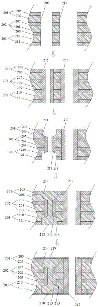
[0018] like figure 2 As shown, the multi-layer PCB board includes a first back-drilling layer 201 , a second back-drilling layer 203 and a laminated layer 202 disposed between the first back-drilling layer 201 and the second back-drilling layer 203 . Wherein, the first backdrilling layer...

Embodiment 2

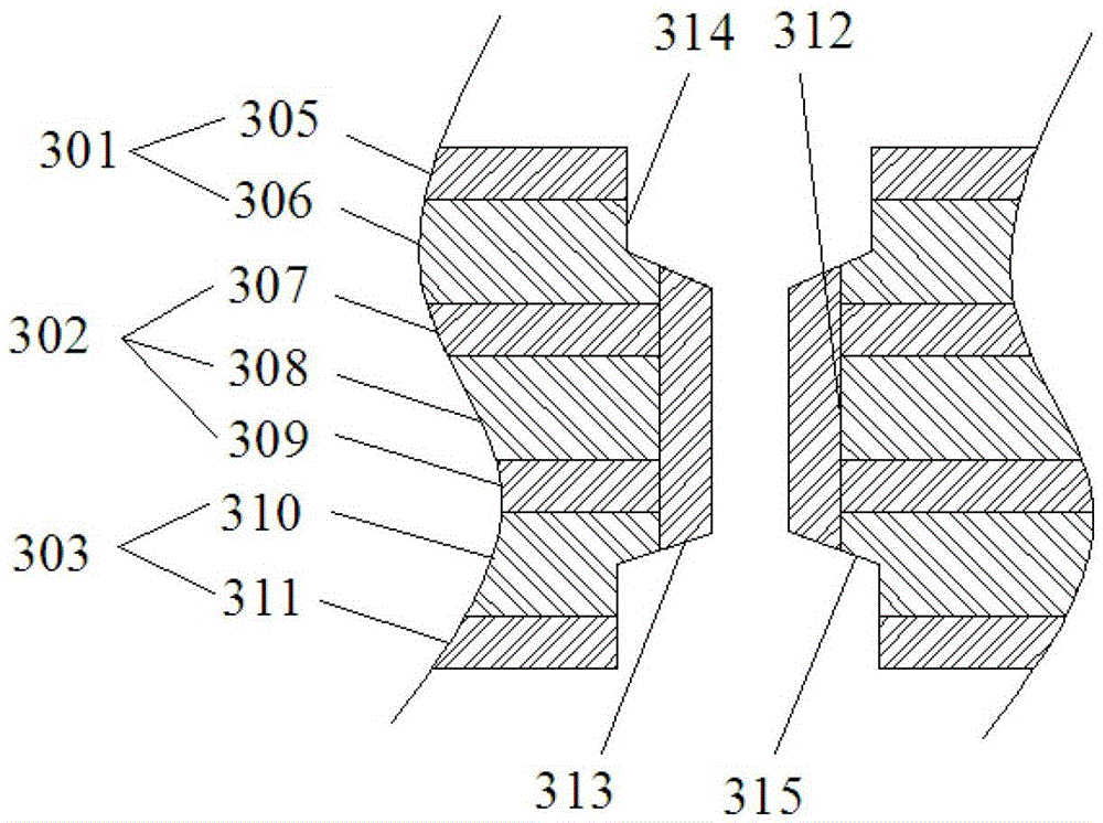
[0032] like image 3As shown, a multilayer PCB board includes a first back drill layer 301 with at least one outer conductive layer, a second back drill layer 303 with at least one outer conductive layer and a A laminated layer 302 having at least two circuit layers between the drill layer and the second back-drill layer. Wherein, the first backdrilling layer 301 includes a first insulating layer 306 and a first metal layer 305 disposed on the first insulating layer 306; The second metal layer 307 and the third metal layer 309 disposed on the lower surface of the second insulating layer 308; the second backdrilling layer 303 includes a third insulating layer 310 and a fourth metal layer 311 disposed on the lower surface of the third insulating layer 310 . The first back-drilled layer 301 is provided with a first back-drilled hole 314 , and the second back-drilled layer 303 is provided with a second back-drilled hole 315 opposite to the first back-drilled hole 314 . The lami...

Embodiment 3

[0035] like Figure 4 As shown, a multilayer PCB board includes a first back drill layer 401 with at least one outer conductive layer, a second back drill layer 403 with at least one outer conductive layer and a A laminated layer 402 having at least two circuit layers between the drill layer and the second back-drill layer. Wherein, the first backdrilling layer 401 includes a first insulating layer 406 and a first metal layer 405 disposed on the first insulating layer 406; The second metal layer 407 and the third metal layer 409 disposed on the lower surface of the second insulating layer 408; the second backdrilling layer 403 includes a third insulating layer 410 and a fourth metal layer 411 disposed on the lower surface of the third insulating layer 410 . The first back-drilling layer 401 is provided with a first back-drilling hole 414 , and the second back-drilling layer 403 is provided with a second back-drilling hole 415 opposite to the first back-drilling hole 414 . T...


PUM


Abstract

The invention discloses a method for manufacturing a multilayer PCB board, which mainly includes: drilling a first through hole on a multilayer PCB board, and metallizing the first through hole to form a first hole wall on the first through hole wall. Conductive layer; perform first backdrilling on the first backdrilling layer along the metallized first through hole to remove part of the first conductive layer located on the first backdrilling layer; on the second backdrilling layer A second back-drilling is performed along the metallized first through hole to remove part of the first conductive layer on the second back-drilled layer. The invention also provides a corresponding multi-layer PCB board. The method of the present invention is by making conductive through-hole on multi-layer PCB board, and removes the part conductive layer of conductive through-hole with the mode of back-drilling, so that the conductive through-hole after back-drilling only connects the conductive layer of lamination, and does not connect with back-drilling. The conductive layer of the drilling layer is disconnected, which realizes the connection between the conductive layers of the stacked layers of the multi-layer PCB board, improves the production efficiency, and reduces the difficulty of alignment.

Description

technical field [0001] The invention relates to the field of electronic devices, in particular to a method for manufacturing a multilayer PCB board and the multilayer PCB board. Background technique [0002] At present, the connection between inner-layer boards and inner-layer boards of a multilayer printed circuit board (PCB, Printed Circuit Board) is realized by making inner-layer metallized holes in the inner-layer board. Specifically, according to the traditional manufacturing process of buried blind vias, two or more layers of inner layer boards to be connected are usually pressed together first, then through holes are drilled on the inner layer boards, and then electroplated to form inner layer metallized holes to realize inner layer metallization. The connection between the layer board and the inner layer board, and then press the upper and lower outer layer boards and the lower outer layer board on the inner layer board to make a multi-layer PCB board with conductive...

Claims


Application Information

Patent Timeline
Patent Type & Authority Patents(China)
IPC IPC(8): H05K3/46H05K1/02
Inventor 雍慧君
Owner SHENNAN CIRCUITS
Why Eureka
Try Eureka