An infrared imaging detection chip based on wave vector measurement
An infrared imaging and chip technology, applied in the direction of electric radiation detectors, etc., to achieve the effects of high structural stability, large measurable range, and high measurement accuracy
- Summary
- Abstract
- Description
- Claims
- Application Information
AI Technical Summary
Problems solved by technology
Method used
Image
Examples
Embodiment Construction
[0024] In order to make the object, technical solution and advantages of the present invention more clear, the present invention will be further described in detail below in conjunction with the accompanying drawings and embodiments. It should be understood that the specific embodiments described here are only used to explain the present invention, not to limit the present invention. In addition, the technical features involved in the various embodiments of the present invention described below can be combined with each other as long as they do not constitute a conflict with each other.
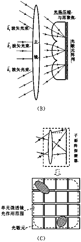
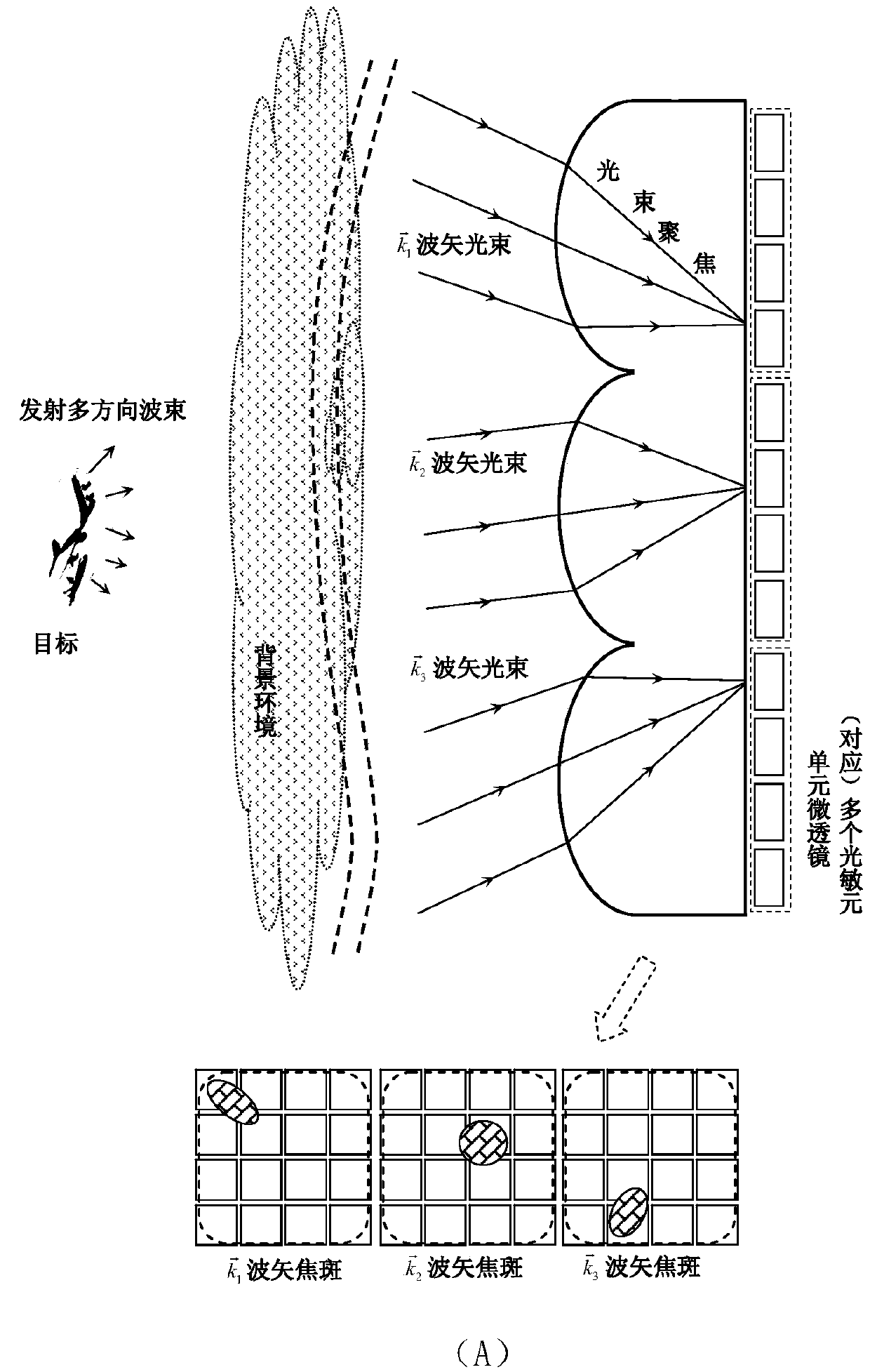
[0025]Generally speaking, the infrared outgoing light wave of the target spreads and propagates in a gradually increasing airspace. The difference in energy transfer efficiency of beams with different wave vector directions reflects the property that the ability of the target or its different parts to project infrared energy to the surrounding airspace is different, which can be attributed to...
PUM
 Abstract
Description
Claims
Application Information


