Method for manufacturing low-reflectivity pattern sapphire substrate

A sapphire substrate and graphic substrate technology, applied in electrical components, circuits, semiconductor devices, etc., can solve the problems of lack of international competitiveness, insufficient research and development of high-end products, and monopoly of high-end markets.

Inactive Publication Date: 2014-02-12
INST OF SEMICONDUCTORS - CHINESE ACAD OF SCI
View PDF3 Cites 3 Cited by
  • Summary
  • Abstract
  • Description
  • Claims
  • Application Information

AI Technical Summary

Problems solved by technology

At present, my country's semiconductor lighting industry has a certain foundation, but the research and development of high-end products is insufficient, lacking international competitiveness, and the high-end market is monopolized by large foreign companies

Method used


Image

  • Method for manufacturing low-reflectivity pattern sapphire substrate
  • Method for manufacturing low-reflectivity pattern sapphire substrate
  • Method for manufacturing low-reflectivity pattern sapphire substrate

Examples


Embodiment Construction

[0024] In order to make the object, technical solution and advantages of the present invention clearer, the present invention will be described in further detail below in conjunction with specific embodiments and with reference to the accompanying drawings.

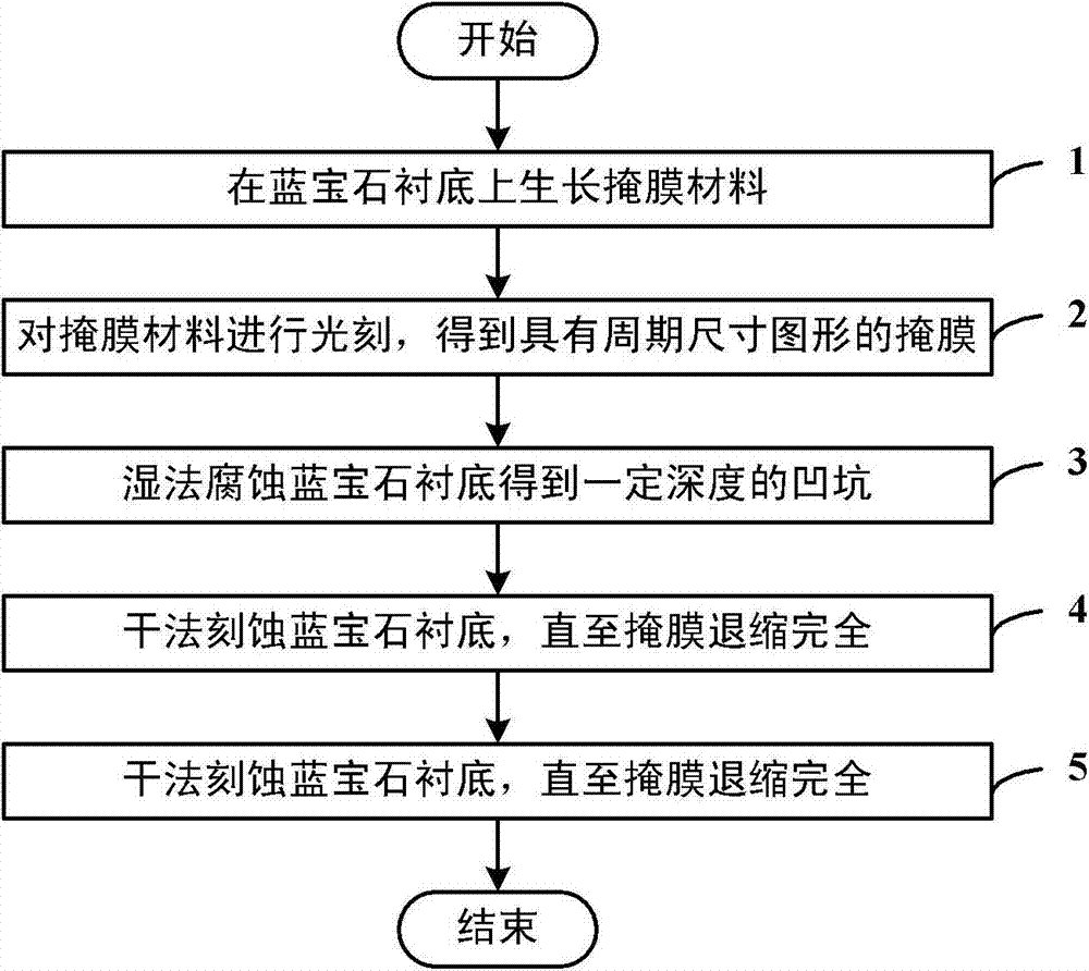
[0025] The key of the present invention is to prepare the sapphire pattern substrate by combining dry and wet etching, select appropriate ICP etching conditions to form periodic patterning on the sapphire surface, and effectively reduce the direct reflection of light. After the material is grown, the loss of light in the material can be effectively reduced, and the extraction efficiency and output rate of light can be improved to improve the luminous efficiency of the chip.

[0026] Such as figure 1 as shown, figure 1 It is a flow chart of a method for preparing a low-reflectivity sapphire pattern substrate provided by the present invention, the method comprising:

[0027] Step 1: growing a mask material on a sapphire s...


PUM


Abstract

The invention discloses a method for manufacturing a low-reflectivity pattern sapphire substrate. The method includes the steps that a mask material grows on a sapphire substrate; photoetching is carried out on the mask material to obtain a mask with a periodical size pattern; wet etching is carried out on the sapphire substrate to acquire pits with certain depths; dry etching is carried out on the sapphire substrate till the mask shrinks completely; surface cleaning is carried out. According to the method for manufacturing the low-reflectivity pattern sapphire substrate by combining the dry method and the wet method, wet etching is carried out on the sapphire substrate first under the condition that the mask is not consumed, then, dry etching is carried out on the sapphire substrate, the utilization ratio of the mask is greatly improved, the periodic pattern formed through the method can be deeper than a pattern in the same period, and therefore the purpose of low reflectivity is achieved.

Description

technical field [0001] The invention relates to the technical field of semiconductors, in particular to a method for preparing a low reflectivity sapphire pattern substrate. Background technique [0002] Semiconductor lighting is another revolution in lighting sources after incandescent lamps and fluorescent lamps. Semiconductor lighting technology develops rapidly, has a wide range of application fields, strong industrial driving force, and great energy-saving potential. It is recognized as one of the most promising high-tech energy-saving industries. [0003] Semiconductor lighting products with GaN LED as the core have the advantages of high luminous efficiency, energy saving, long life, and environmental protection. At present, my country's semiconductor lighting industry has a certain foundation, but the research and development of high-end products is insufficient, lacking international competitiveness, and the high-end market is monopolized by large foreign companies...

Claims


Application Information

Patent Timeline
Patent Type & Authority Applications(China)
IPC IPC(8): H01L33/00
CPCH01L33/0093
Inventor 黄亚军樊中朝王莉季安
Owner INST OF SEMICONDUCTORS - CHINESE ACAD OF SCI
Why Eureka
Try Eureka