Transistor and transistor array

A technology of transistors and transistor units, applied in the direction of electric solid devices, semiconductor devices, piezoelectric devices/electrostrictive devices, etc., can solve the problems of high design and manufacturing difficulty, inability to realize, application and other problems

Active Publication Date: 2014-02-12
BEIJING INST OF NANOENERGY & NANOSYST
View PDF4 Cites 24 Cited by
  • Summary
  • Abstract
  • Description
  • Claims
  • Application Information

AI Technical Summary

Problems solved by technology

Although this single-channel field-effect transistor based on semiconductor nanowires uses the semiconductor nanowires to control the carrier transport process in the device, it still needs Applied voltage
Therefore, the structure of th

Method used


Image

  • Transistor and transistor array
  • Transistor and transistor array
  • Transistor and transistor array

Examples


Embodiment 1

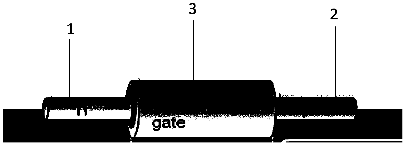
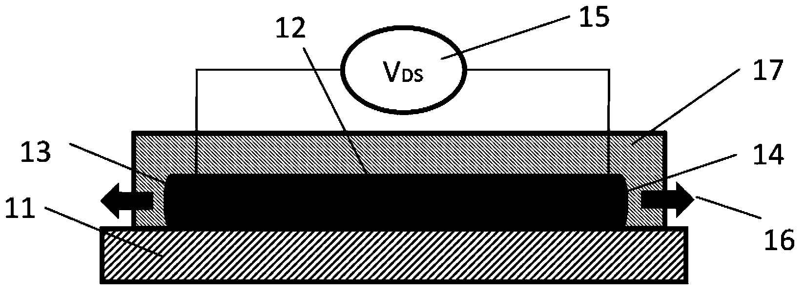
[0049] In this embodiment, the transistor is arranged on the substrate, the connection line between the first electrode and the second electrode is basically parallel to the substrate, and the piezoelectric body is a bulk material, see figure 2 , the transistor is disposed on the substrate 11, the substrate 11 includes a first electrode 13 of the transistor, a piezoelectric body 12 and a second electrode 14, the first electrode 13 and / or the second electrode 14 are used to apply strain to the piezoelectric body 12, Stress or pressure16. Wherein, the piezoelectric body 12 is a bulk material, which may be a bulk material with a wurtzite structure, a bulk material with a sphalerite structure, a bulk material with a lithium niobate structure, or a bulk material with semiconductor properties, such as ZnO, GaN, CdS, InN, InGaN, CdTe, CdSe or ZnSnO 3 and other materials. In this embodiment, the preparation method of the piezoelectric body is to selectively deposit the material of ...

Embodiment 2

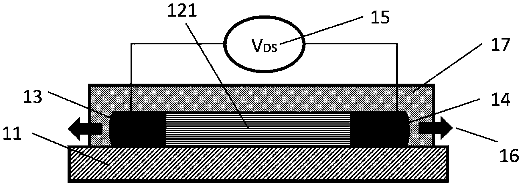
[0056] The difference between this embodiment and Embodiment 1 is that the piezoelectric body of the transistor is a one-dimensional piezoelectric structure, and the one-dimensional piezoelectric structure may include piezoelectric nanowires, nanowires, nanorods, nanocolumns or nanobelts. . In this embodiment, the number of one-dimensional piezoelectric structures is not limited, and it may be one one-dimensional piezoelectric structure, such as a nanowire or nanorod, or multiple one-dimensional piezoelectric structures arranged in parallel, such as multiple parallel arrayed nanowires or nanorods. see image 3 , the piezoelectric bodies 121 are nanowires or nanorods arranged in parallel, the first electrode 13 and the second electrode 14 are oppositely arranged at the two ends of the nanowire or nanorod, and the first electrode 13 and / or the second electrode 14 is used to apply strain or stress to the piezoelectric body; the material of the piezoelectric body 121 produces a ...

Embodiment 3

[0061] The difference between this embodiment and Embodiment 1 and Embodiment 2 is that the piezoelectric body of the transistor is a piezoelectric film, see Figure 4 , the piezoelectric body 122 is a piezoelectric film, and the piezoelectric body 122 shown in the figure is a piezoelectric film cross section. The first electrode 13 and the second electrode 14 are oppositely arranged at two ends of the piezoelectric film or piezoelectric nanoribbon.

[0062] The piezoelectric body 122 is a piezoelectric film, the connecting line of the first electrode 13 and the second electrode 14 is substantially parallel to the surface of the piezoelectric film, and the first electrode 13 and the second electrode 14 are connected to the two end faces of the piezoelectric film (That is, the piezoelectric film between the first electrode and the second electrode is a piezoelectric body 122 ), the size of the first electrode 13 and the second electrode 14 should be at least equivalent to the t...


PUM

PropertyMeasurementUnit
Thicknessaaaaaaaaaa

Abstract

The invention provides a transistor which comprises a piezoelectric crystal, a first electrode and a second electrode. The first electrode and the second electrode are oppositely arranged at the two ends of the piezoelectric crystal respectively. The first electrode and/or the second electrode are/is used for exerting strain or stress on the piezoelectric crystal. Materials of the piezoelectric crystal have the piezoelectric effect under the action of the strain or the stress. Correspondingly, the invention further provides a transistor array. Strain or stress or pressure is exerted on the electrode of one end of the piezoelectric crystal, so that the piezoelectric crystal correspondingly deforms, the interface barrier between the piezoelectric crystal materials and electrode materials can be effectively regulated by generated piezoelectric potential, and the function similar to grid voltage in a field effect transistor is achieved. The transistor or the transistor array can be applied to the fields of micro-nano electromechanical systems, nano-robots, human-computer interaction interfaces, flexible sensors and the like.

Description

technical field [0001] The invention relates to the field of semiconductor devices, in particular to a transistor and a transistor array applied in the fields of micro-nano electromechanical systems, nano-robots, human-computer interaction interfaces, bendable sensors, and the like. Background technique [0002] Among the traditional electronic devices based on semiconductor nanowires, the single-channel field-effect transistor (FET) is the most researched, and its structure is shown in figure 1 , wherein the source 1 and the drain 2 are located at both ends of the nanowire, and the gate 3 wound around the nanowire applies a voltage to the nanowire channel. Apply an external voltage V between source 1 and drain 2 DS , the carrier transport process in semiconductor devices is regulated or triggered by the gate voltage. Although this single-channel field-effect transistor based on semiconductor nanowires uses the semiconductor nanowires to control the carrier transport proce...

Claims


Application Information

Patent Timeline
IPC IPC(8): H01L41/08H01L27/20
Inventor 王中林
Owner BEIJING INST OF NANOENERGY & NANOSYST
Why Eureka
Try Eureka