
Detection method for chip defect

A detection method and chip defect technology, which is applied in the direction of measuring devices, material analysis through optical means, instruments, etc., can solve the problems of low chip defect detection accuracy and achieve the effect of improving accuracy

Inactive Publication Date: 2014-02-26
SHANGHAI HUALI MICROELECTRONICS CORP
View PDF13 Cites 9 Cited by
  • Summary
  • Abstract
  • Description
  • Claims
  • Application Information

AI Technical Summary

Problems solved by technology

[0008] In view of the above existing problems, the present invention discloses a defect detection method to overcome the problem in the prior art that optical defect detection concentrates the focal length of the optical path at a certain height, resulting in low detection accuracy of chip defects

Method used


Image

  • Detection method for chip defect
  • Detection method for chip defect
  • Detection method for chip defect

Examples


Embodiment 1

[0043] Such as Figure 5 , Figure 7-Figure 11 The detection method of chip defect shown:

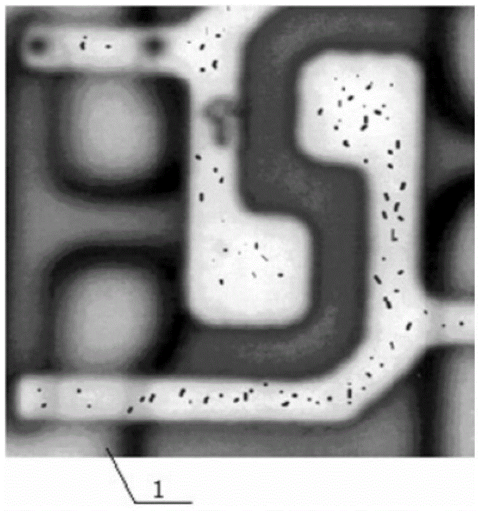
[0044] First provide a chipset and an optical inspection equipment, such as Figure 5 As shown, there are defects on the top and bottom of the chipset's circuit4, the optical inspection equipment is aimed at Figure 5 The defect 4 shown is tested;

[0045] Establish defect scanning procedures, for example Picture 9 The initial scan is set to the first focal length value above the circuit. When the optical detection device performs the initial scan, the first signal image of the chipset is collected, and the optical detection device converts the first signal image Is the first data image and stored in the database;

[0046] Right as Picture 10 The return scan shown is to set the second focal length value at the bottom of the circuit. When the optical detection device performs the return scan, the second signal image of the chipset is collected, and the second signal image is captured by the o...

Embodiment 2

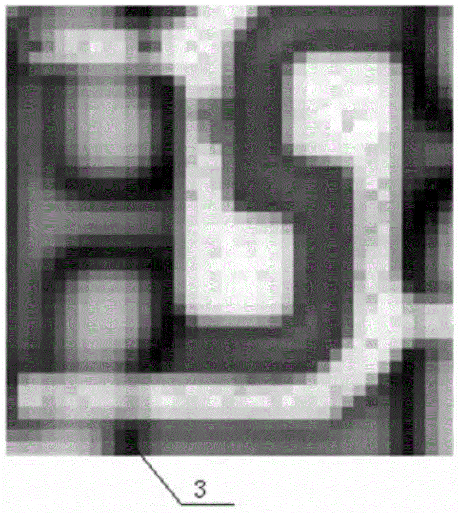
[0050] Such as Picture 12 with 13 Shown: This embodiment is roughly the same as the first embodiment, and the specific improvement is as follows: Picture 12 As shown in the defect 4 located on the top and middle of the circuit, establish a scanning program for defect detection, set the first focus value on the circuit for the initial scan of the chip, and set the second focus on the middle of the circuit for the return scan of the chip Value, which can accurately detect defects above and in the middle of the circuit in the chip.

[0051] In the above two embodiments, the light detection device can set different focal lengths to perform multiple round-trip scans on the chip, and superimpose the two focal length data images of each round-trip scan, and combine the superimposed data image with the chip's Normal data images are compared, that is, multiple round-trip scanning is performed for multiple comparisons, so that defects in the chip can be detected more accurately.

[0052] I...


PUM


Abstract

A disclosed detection method for chip defect comprises the following steps: providing a chipset and an optical detection apparatus; setting a first focal length value, employing the first focal length value and performing initial scan on the chipset by the optical detection apparatus, and storing the initial scan result in a database; setting a second focal length value, employing the second focal length value and performing return scan on the chipset by the optical detection apparatus, and storing the return scan result in the database; and superposing the initial scan result and the return scan result in the database, comparing the superposed scan result and a normal scan result of a chip to determine the position of the defect. The detection method for the chip defect helps to improve the detection precision on the chip defect, and is simple and convenient to operate, thereby improving the detection efficiency on the chip defect.

Description

Technical field [0001] The invention relates to the field of semiconductor manufacturing, in particular to a method for detecting chip defects. Background technique [0002] The advanced integrated circuit manufacturing process generally includes several hundred steps. A small error in any link will lead to the failure of the entire chip. Especially as the critical size of the circuit continues to shrink, its requirements for process control become stricter. In order to find and solve problems in time during the production process, optical inspection equipment is generally configured to inspect products online. [0003] The working principle of chip defect detection is to convert the optical image on the chip into a data image represented by different light and dark gray scales. Figure 1a-1c It is a schematic diagram of converting an optical image of a circuit into a data image in the background of the present invention, such as Figure 1a-1c As shown, the optical signal transmittin...

Claims


Application Information

Patent Timeline
IPC IPC(8): G01N21/956
Inventor 倪棋梁陈宏璘龙吟
Owner SHANGHAI HUALI MICROELECTRONICS CORP
Learn More