

Printed circuit board
A printed circuit board and current technology, used in printed circuit parts, static electricity, electrical components, etc., can solve problems such as electrostatic shock and damage, and achieve the effects of cost control, simple processing technology and wide application range.
- Summary
- Abstract
- Description
- Claims
- Application Information
AI Technical Summary
Problems solved by technology
Method used
Image

Examples
Embodiment 1
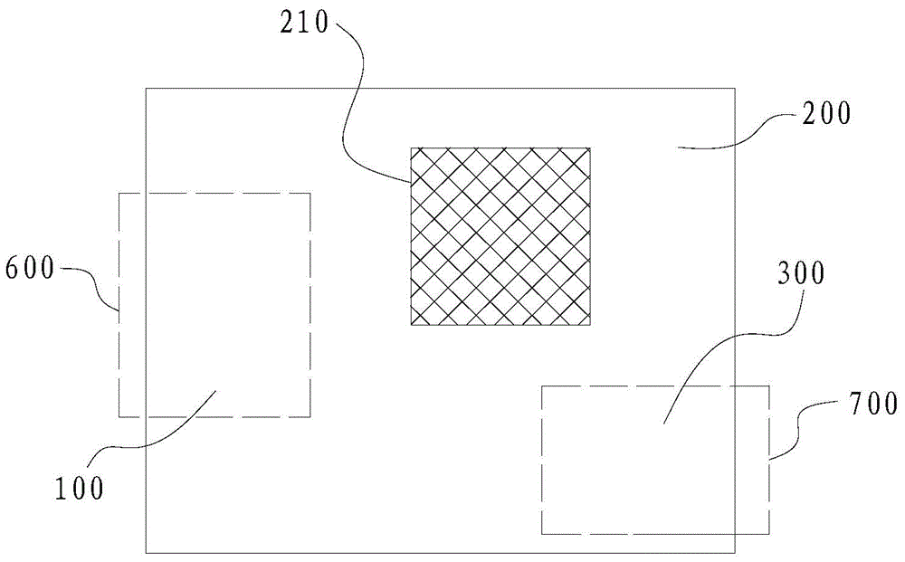
[0029] see figure 2 , this embodiment provides a printed circuit board, the printed circuit board has a shield ground 100, a system ground 200 and a power ground 300, the printed circuit board is also provided with a groove 400 capable of blocking current, the groove The slot 400 is located between the shielding ground 100 and the system ground 200, and is used to realize the isolation between the shielding ground 100 and the system ground 200, block the current on both sides of the trench 400, and be used for Guide the flow of static electricity; the power supply ground 300 is connected to the shielding ground 100 and the system ground 200 respectively. Usually, at least one component 210 is arranged on the system ground 200, such as a CPU module, etc. According to different circuit board functions, the system ground 200 can be any one of digital signal ground and analog signal ground; The ground 100 is usually electrically connected to the shielding layers of various exter...
Embodiment 2
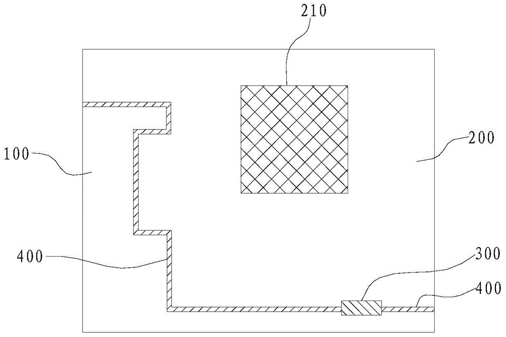
[0035] see image 3 , this embodiment discloses a printed circuit board. This embodiment is another preferred solution for the position of the power ground 300 on the basis of the first embodiment. In addition, other The technical solution also belongs to this embodiment, and will not be described again here.
[0036] Specifically, in order to ensure the best current blocking effect of the trench 400, the power ground 300 may also be located at the boundary of the printed circuit board, one end of the trench 400 is connected to the power ground 300, and the other One end extends to a corresponding border of the printed circuit board. That is to say, the trench 400 and the power ground 300 are connected together to complete the separation of the shielding ground 100 and the system ground 200, wherein the trench 400 is used to block the The current between the shielding ground 100 and the system ground 200 , wherein the power supply ground 300 is used to conduct the shielding ...
Embodiment 3
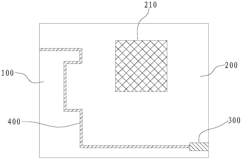
[0039] see Figure 4 , this embodiment discloses a printed circuit board. This embodiment is another preferred solution for the position of the power ground 300 on the basis of the first embodiment. In addition, other The technical solution also belongs to this embodiment, and will not be described again here.
[0040]Specifically, the power ground 300 of this embodiment is located at the boundary of the printed circuit board, one end of the groove 400 is adjacent to but not in contact with the power ground 300, and the other end extends to the edge of the printed circuit board. corresponding boundaries. That is to say, there is a disconnection area 500 between one end of the trench 400 adjacent to the power ground 300 and the boundary adjacent to the end, and the shielding ground 100 and the system in the disconnection area 500 The ground 200 is connected, the power ground 300 is located in the disconnected area 500, and the power ground 300 is not connected to the boundary...
PUM
 Abstract
Description
Claims
Application Information