A kind of embedded chip and its preparation method

An embedded, chip technology, used in semiconductor/solid-state device manufacturing, semiconductor/solid-state device components, semiconductor devices, etc., can solve the problems of chip damage, static electricity, damage, etc. The effect of antistatic ability

Active Publication Date: 2022-04-12
SHENNAN CIRCUITS
View PDF0 Cites 0 Cited by
  • Summary
  • Abstract
  • Description
  • Claims
  • Application Information

AI Technical Summary

Problems solved by technology

In addition, embedding bare chips is usually to complete the embedding of multiple bare chips on a whole substrate. After the bare chips are embedded, each chip is then cut to obtain the required one or more embedded chips. , however, static electricity is usually generated during dicing, which can cause damage to embedded chips
In addition, the chip pins of the cut chips are separated from each other, and may be damaged by static electricity during storage

Method used


Image

  • A kind of embedded chip and its preparation method
  • A kind of embedded chip and its preparation method
  • A kind of embedded chip and its preparation method

Examples


Embodiment Construction

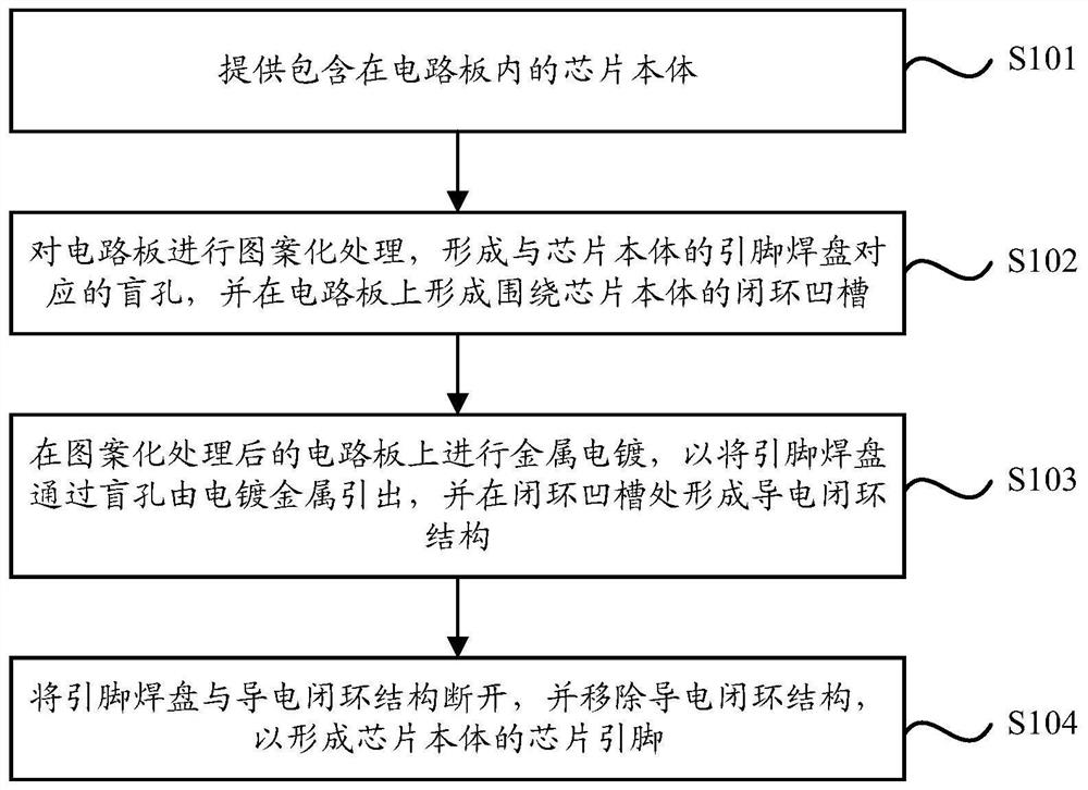
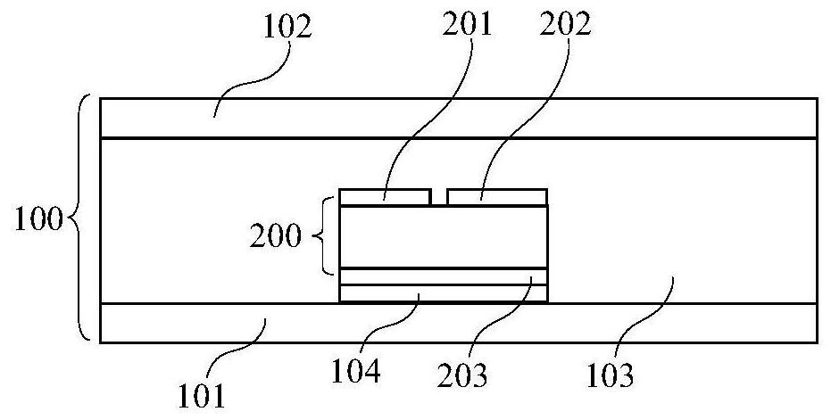
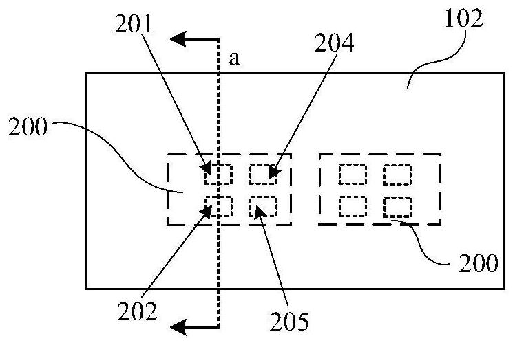
[0070] The following will clearly and completely describe the technical solutions in the embodiments of the present invention with reference to the accompanying drawings in the embodiments of the present invention. Obviously, the described embodiments are only some, not all, embodiments of the present invention. Based on the embodiments of the present invention, all other embodiments obtained by persons of ordinary skill in the art without making creative efforts belong to the protection scope of the present invention.

[0071] It should be noted that if there is a directional indication (such as up, down, left, right, front, back...) in the embodiment of the present invention, the directional indication is only used to explain the position in a certain posture (as shown in the accompanying drawing). If the specific posture changes, the directional indication will also change accordingly.

[0072] In addition, if there are descriptions involving "first", "second" and so on in ...


PUM


Abstract

The invention provides an embedded chip and a preparation method thereof. The embedded chip includes a circuit board on which electroplated metal is arranged; a chip body located inside the circuit board, and the chip body has a plurality of solder pins a disc, the plurality of pin pads are led out from the electroplated metal to form a plurality of chip pins; and a conductive insert, which is detachably inserted into the plurality of chip pins. By providing the embedded chip with a conductive insert that can be detachably plugged with its chip pins, the chip pins are connected to each other through the conductive insert during the placement and movement of the embedded chip, thereby improving the resistance of the chip. Electrostatic capability, to achieve electrostatic protection of the chip, just remove the conductive plug-in when the embedded chip needs to be used.

Description

technical field [0001] The invention relates to the technical field of semiconductor chips, in particular to an embedded chip and a preparation method thereof. Background technique [0002] With the development of the information society, the amount of information processed by various electronic devices is increasing day by day, and the demand for high-frequency and high-speed signal transmission is increasing day by day. Embedding the semiconductor chip in the circuit board for packaging can effectively shorten the connection distance between the semiconductor chip and the packaging substrate, and provide a strong guarantee for high-frequency and high-speed signal transmission. Bare chips embedded in circuit boards can also meet the development needs of high integration of packages and miniaturization of electronic products. [0003] In the prior art, the bare chip is usually prepared for embedding the circuit board by attaching the bare chip to the circuit board, and the ...

Claims


Application Information

Patent Timeline
Patent Type & Authority Patents(China)
IPC IPC(8): H01L23/488H01L23/49H01L23/60H01L21/48
CPCH01L23/488H01L23/49H01L23/60H01L21/4814H01L21/4885H01L2224/18
Inventor 黄立湘缪桦
Owner SHENNAN CIRCUITS
Why Eureka
Try Eureka