

An electrostatic protection circuit, semiconductor integrated circuit device and electronic equipment
A technology for protecting circuits and electrostatic protection, which is applied in the field of electronic equipment and semiconductor integrated circuit devices, and can solve the problems of complex use environment, reduction of the characteristic size of semiconductor integrated circuits, damage to semiconductor integrated circuit devices, etc., to achieve electrostatic protection and avoid damage Effect
- Summary
- Abstract
- Description
- Claims
- Application Information
AI Technical Summary
Problems solved by technology
Method used
Image

Examples
Embodiment Construction
[0035] In order to make the purpose, technical solutions and advantages of the present invention clearer, the implementation method of the present invention will be described in detail below in conjunction with the accompanying drawings and embodiments, so as to solve technical problems and achieve technical effects by applying technical means to the present invention. The process is well understood and implemented accordingly.
[0036] In the following description, many specific details are set forth in order to fully understand the present invention. However, the present invention can also be implemented in other ways different from those described here. Therefore, the protection scope of the present invention is not limited by the specific details disclosed below. EXAMPLE LIMITATIONS.
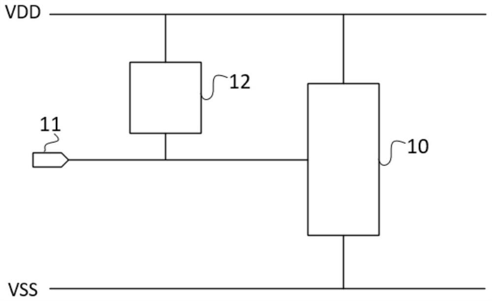
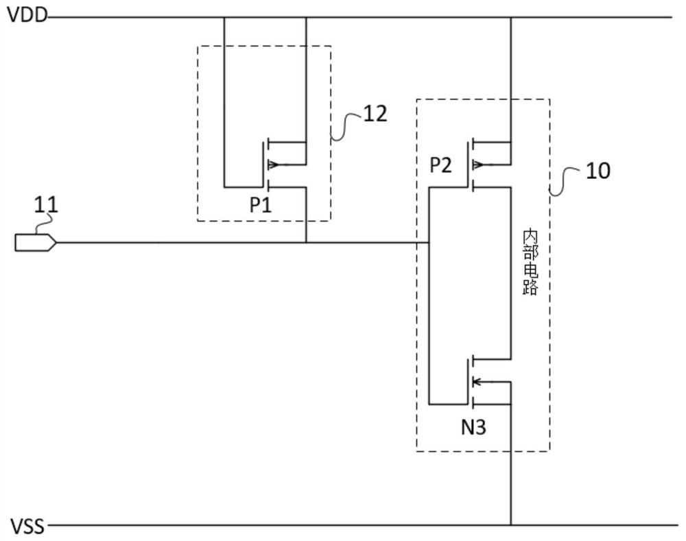
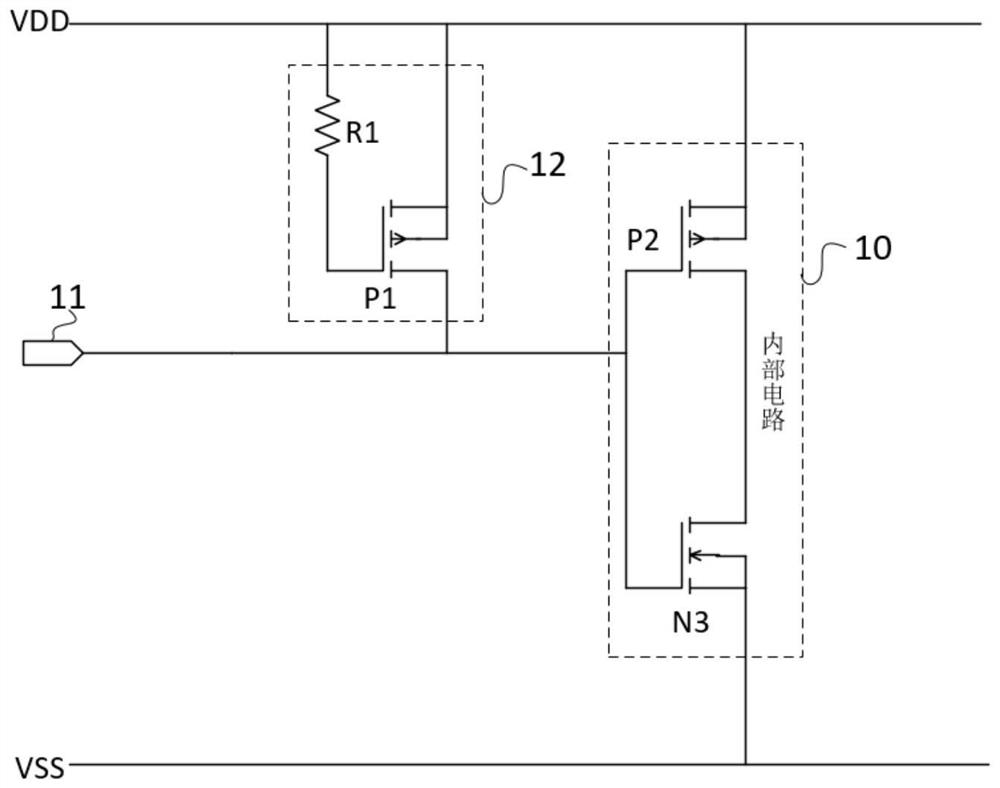
[0037] According to an embodiment of the present invention, an electrostatic protection circuit is provided, figure 1 A schematic structural diagram of an electrostatic protection circuit p...
PUM
 Abstract
Description
Claims
Application Information