PCB electroplating method for improving electroplating uniformity

A uniformity, PCB board technology, applied in the field of PCB processing, can solve the problems of etching difficulties, uneven plating, etc., to achieve the effect of improving uniformity, precise transmission, and solving difficulties in plating and etching

Active Publication Date: 2014-03-05
SHENZHEN KINWONG ELECTRONICS
View PDF3 Cites 24 Cited by
  • Summary
  • Abstract
  • Description
  • Claims
  • Application Information

AI Technical Summary

Problems solved by technology

[0006] In view of the shortcomings of the above-mentioned prior art, the purpose of the present invention is to provide a PCB electroplating method for improvin

Method used


Image

  • PCB electroplating method for improving electroplating uniformity
  • PCB electroplating method for improving electroplating uniformity
  • PCB electroplating method for improving electroplating uniformity

Examples


Embodiment Construction

[0023] The present invention provides a PCB electroplating method for improving the uniformity of electroplating. In order to make the purpose, technical solution and effect of the present invention clearer and clearer, the present invention will be further described in detail below with reference to the accompanying drawings and examples. It should be understood that the specific embodiments described here are only used to explain the present invention, not to limit the present invention.

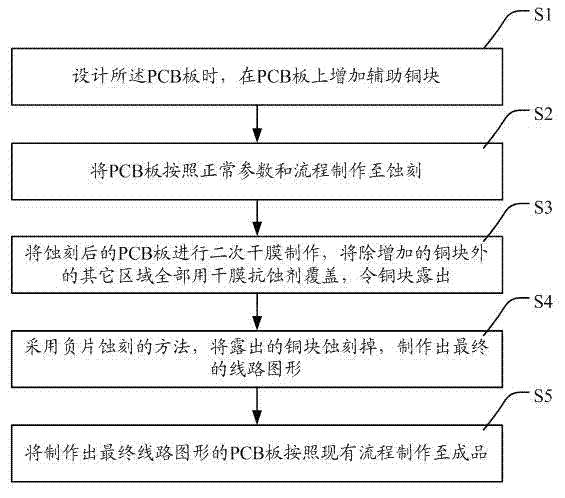
[0024] see figure 1 , which is a flow chart of the PCB electroplating method for improving electroplating uniformity of the present invention. Such as figure 1 As shown, the method includes the following steps;

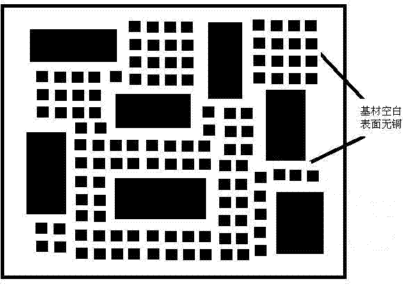
[0025] S1. When designing the PCB board, add an auxiliary copper block on the PCB board;

[0026] S2. Make the PCB board according to the normal parameters and process until it is etched;

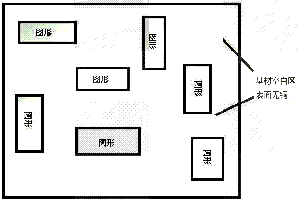
[0027] S3, the etched PCB board is subjected to secondary dry film production, and all ...


PUM


Abstract

The invention discloses a flow diagram of a PCB electroplating method for improving the electroplating uniformity. The PCB electroplating method for improving the electroplating uniformity comprises the steps that firstly, an auxiliary copper block is additionally arranged on a PCB when the PCB is designed; then the PCB is manufactured and etched according to the normal parameters and process; then secondary dry film manufacturing is carried out on the etched PCB, namely all areas, except the area where the copper block is additionally arranged, of the PCB are covered with a dry film photoresist, and the copper block is exposed; the exposed copper block is removed through etching by means of a negative film etching method, and a final circuit graph is formed; the PCB where the final circuit graph is formed is processed according to an existing technological process until a finished product is obtained. By the adoption of the PCB electroplating method for improving the electroplating uniformity, the problem that electroplating and etching are difficult due to the uneven electroplating of a PCB with graphs distributed in an isolated mode is solved, the uniformity of the thickness of electroplating copper of the PCB is improved, and therefore signals can be transmitted more accurately when a user uses the PCB.

Description

technical field [0001] The invention relates to the technical field of PCB processing, in particular to a PCB electroplating method for improving electroplating uniformity. Background technique [0002] PCB (Printed Circuit Board), the Chinese name is printed circuit board, also known as printed circuit board, printed circuit board, is an important electronic component, a support for electronic components, and a provider of electrical connections for electronic components. Because it is made using electronic printing, it is called a "printed" circuit board. [0003] Due to the current PCB design, the distribution of electroplating patterns is uneven, and there may be only isolated pads or lines locally, while the area of ​​other parts may be too large, or the area of ​​​​the two sides may differ greatly, so that even if the electroplating equipment and solution are good, all parameters are optimal. Conditions, but the actual production of the board may also have uneven plat...

Claims


Application Information

Patent Timeline
IPC IPC(8): H05K3/00
Inventor 张霞陈晓宇
Owner SHENZHEN KINWONG ELECTRONICS
Why Eureka
Try Eureka