
PCB (Printed Circuit Board) bracket for automatic optic inspection device

A PCB board and automatic optical technology, applied in the field of brackets, can solve the problems that the device is easy to be clamped, the detection coverage rate is reduced, and the fixture is easy to be blocked, etc., and the effect of not easy to damage, improving the detection coverage rate, and large clamping space is achieved.

Active Publication Date: 2014-03-12
无锡市同步电子制造有限公司
View PDF11 Cites 4 Cited by
  • Summary
  • Abstract
  • Description
  • Claims
  • Application Information

AI Technical Summary

Problems solved by technology

The automatic optical inspection machine realizes the positioning of the PCB board by clamping the edge of the PCB board with the fixture on the upper part of the working platform. However, when there are devices within 5mm of the edge of the PCB board in this clamping method, it is often difficult to realize the positioning of the PCB board. The positioning of the clamping, the fixture is easy to cover the components on the PCB, thereby reducing the detection coverage, and the components on the PCB are also easily damaged by clamping

Method used


Image

  • PCB (Printed Circuit Board) bracket for automatic optic inspection device

Examples


Embodiment Construction

[0016] The technical solutions of the present invention will be further described below in conjunction with the accompanying drawings and through specific implementation methods.

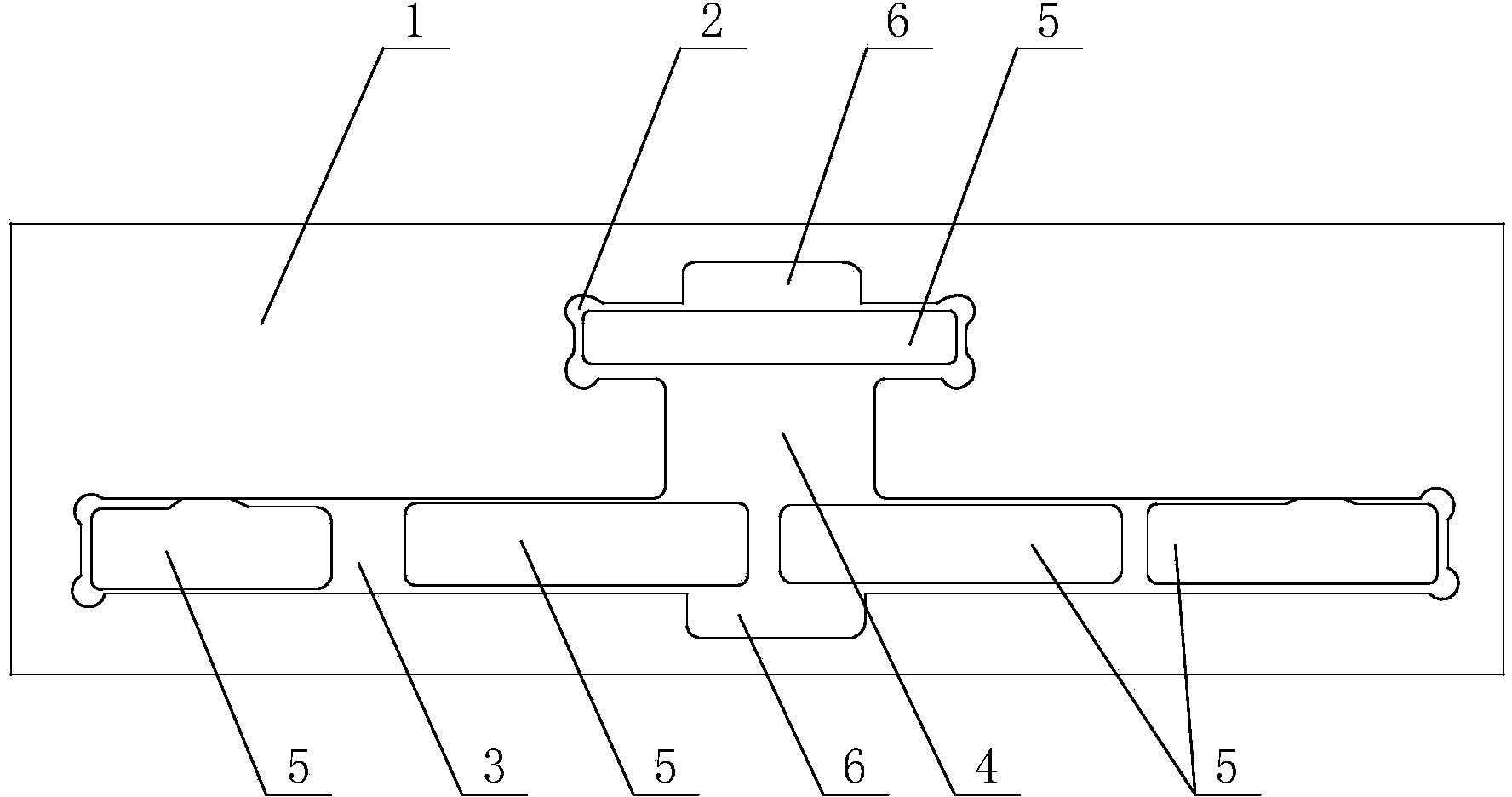
[0017] Please refer to figure 1 as shown, figure 1 It is a structural schematic diagram of a PCB board bracket for an automatic optical inspection machine of the present invention.

[0018] In this embodiment, a PCB board bracket for an automatic optical inspection machine includes a black bracket body 1 made of synthetic stone, and the PCB board is a combination of soft and hard boards, corresponding to the bracket body 1. The upper part is opened with a first cavity 2 for carrying the first hard plate, and the lower part is opened with a second cavity 3 for carrying the second hard plate, and the bracket body 1 is located between the first cavity 2 and the second cavity There is a flexible board cavity 4 for carrying the flexible board between the 3, and the first cavity 2 and the second cavity ...


PUM


Abstract

The invention discloses a PCB bracket for an automatic optic inspection device. The PCB board bracket comprises a bracket main body, wherein a cavity for supporting the PCB is formed in the support main body and matched with the PCB in shape; a through hole for scanning is formed in the cavity. The PCB bracket for the automatic optic inspection device uses the bracket main body to support the PCB, so that the devices on the PCB cannot be shielded after clamping, and the inspection coverage rate is improved; when the PCB is clamped and positioned, the larger clamping space can be achieved, and the devices on the PCB are not easy to be damaged.

Description

technical field [0001] The invention relates to a bracket, in particular to a PCB board bracket for an automatic optical detection machine. Background technique [0002] The automatic optical inspection machine is a device based on optical principles to detect common defects encountered in welding production. During automatic detection, the machine automatically scans the PCB board through the camera, collects images, compares the tested solder joints with the qualified parameters in the database, and checks out the defects on the PCB board through image processing, and detects the defects through the display or automatic marking Displayed and marked out for repair by maintenance personnel. The automatic optical inspection machine realizes the positioning of the PCB board by clamping the edge of the PCB board with the fixture on the upper part of the working platform. However, when there are devices within 5mm of the edge of the PCB board in this clamping method, it is ofte...

Claims


Application Information

Patent Timeline
Patent Type & Authority Applications(China)
IPC IPC(8): G01N21/956
Inventor 应朝晖潘一峰林利剑胡雨佳付建徐杨
Owner 无锡市同步电子制造有限公司
Learn More