Control circuit in power factor correction circuit

A power factor correction and control circuit technology, applied in the direction of output power conversion devices, high-efficiency power electronic conversion, electrical components, etc., can solve the problems of power factor reduction, phase difference, and harmonic content increase, and achieve phase elimination poor effect

Active Publication Date: 2014-03-12
ZHEJIANG YINGFEITE OPTOELECTRONICS CO LTD
View PDF4 Cites 9 Cited by
  • Summary
  • Abstract
  • Description
  • Claims
  • Application Information

AI Technical Summary

Problems solved by technology

This will cause the input current Iin (of the AC input) and the input voltage Vin to have a phase difference in the entire circuit
This is because the input current Iin (of the AC input terminal) of the entire circuit is the sum of the current on the filter capacitor and the input current of the PFC circuit, and the phase of the current on the filter capacitor is 90 degrees ahead of the input voltage, that is, due to the filter capacitor Existence, the phase of the input current Iin is ahead of the phase of the input voltage Vin, so that the phase of the input current Iin and the phase of the input voltage Vin are inconsistent, resulting in a decrease in the power factor of the power supply and an increase in harmonic content

Method used


Image

  • Control circuit in power factor correction circuit
  • Control circuit in power factor correction circuit
  • Control circuit in power factor correction circuit

Examples


Embodiment 1

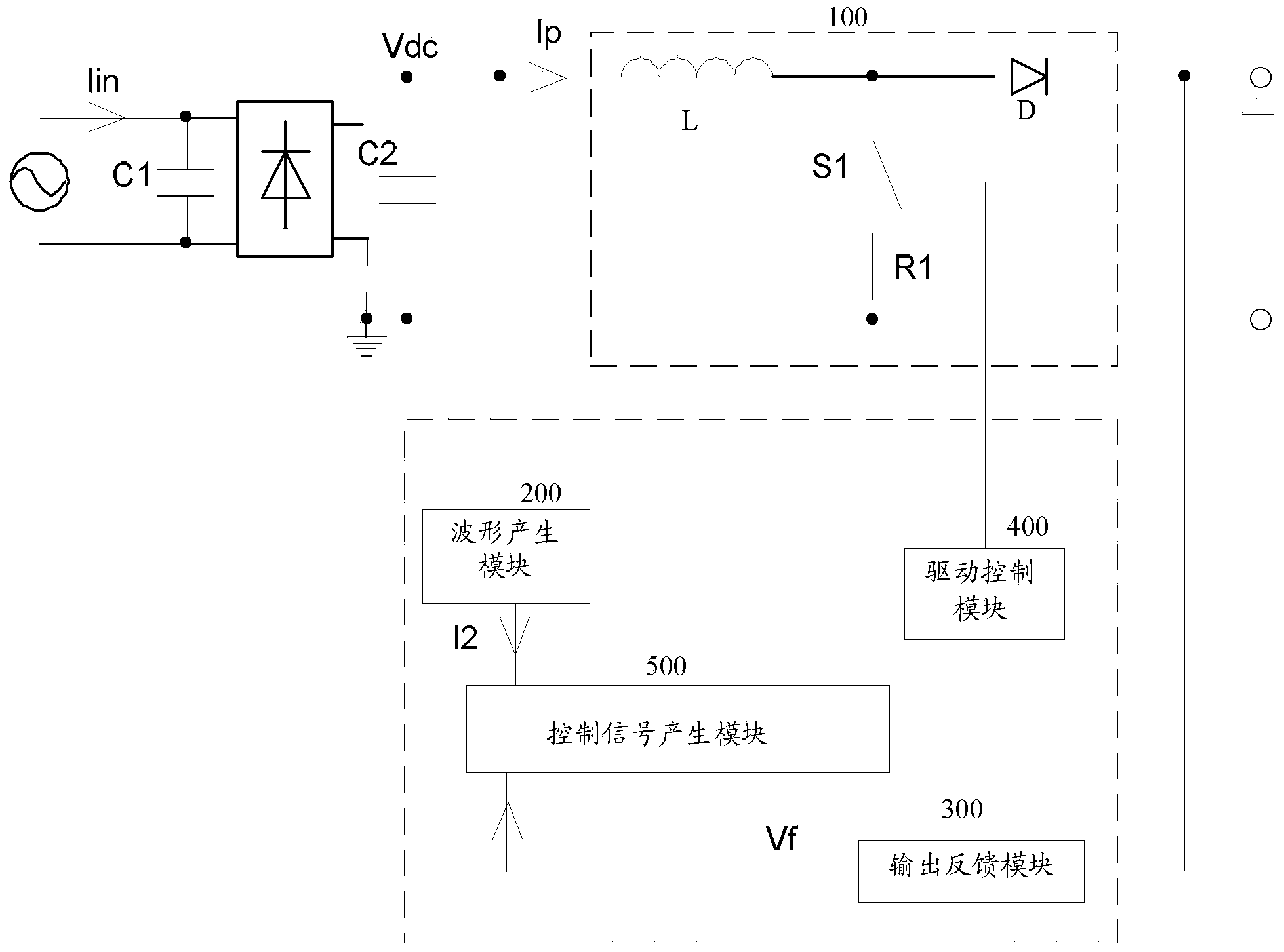
[0053] see figure 2 , which is a schematic diagram of Embodiment 1 of the control circuit in the power factor correction circuit provided by the present invention.

[0054] The control circuit in the power factor correction circuit provided by the embodiment of the present invention includes: a waveform generation module 200, an output feedback module 300, a drive control module 400, and a control signal generation module 500;

[0055] The output feedback module 300 is configured to sample the output electrical parameter of the power factor correction circuit PFC100, compare the sampled output electrical parameter with a preset value, and output a feedback signal Vf according to the comparison result;

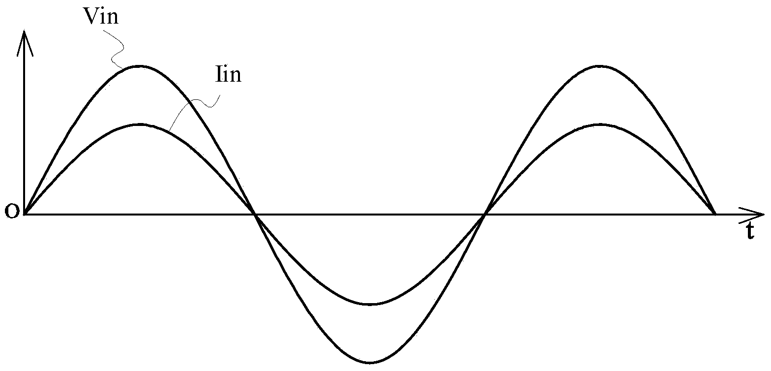
[0056] It should be noted that the electrical parameter output by the power factor correction circuit PFC100 may be a voltage signal or a current signal.

[0057] It should be noted that, the PFC circuit 100 in this embodiment takes a Boost circuit as an example, as figure ...

Embodiment 2

[0068] The following mainly introduces the control signal generation module provided by the embodiment of the present invention with reference to the accompanying drawings.

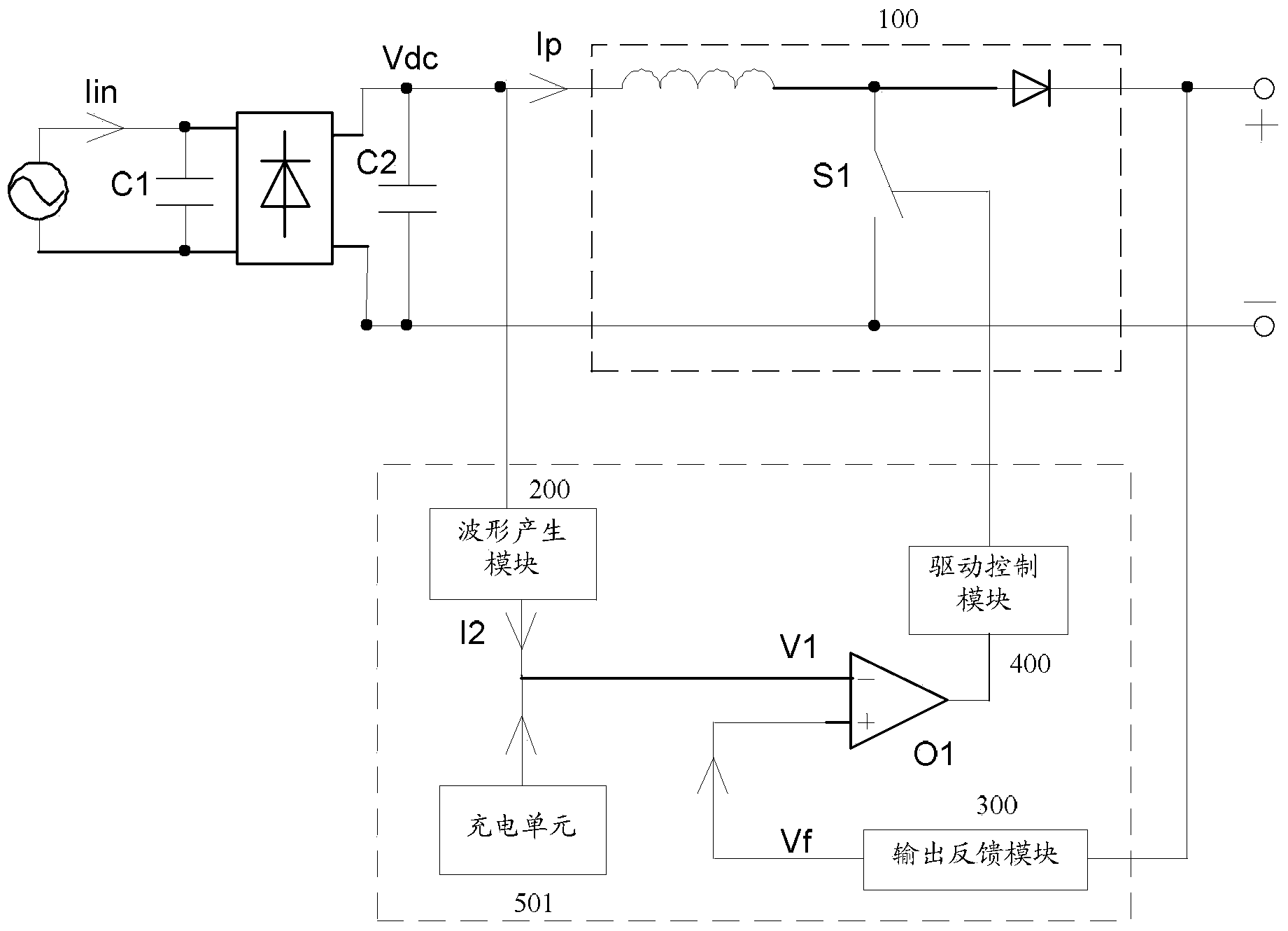
[0069] see image 3 , which is a schematic diagram of Embodiment 2 of the control circuit in the power factor correction circuit provided by the present invention.

[0070] The control signal generating module provided in this embodiment includes: a charging unit 501 and a comparator O1;

[0071] The charging unit 501 includes a current source Id and a capacitor Ct; for details, see Figure 4c .

[0072] The current source Id and the second signal I2 charge the capacitor Ct;

[0073] The voltage on the capacitor Ct is input to an input terminal of the comparator O1;

[0074] The feedback signal Vf is input to the other input terminal of the comparator O1;

[0075] The output terminal of the comparator O1 outputs the control signal to the driving control module 400 .

[0076] The drive control module...

Embodiment 3

[0109] see Figure 6 , which is a schematic diagram of Embodiment 3 of the control circuit in the power factor correction circuit provided by the present invention.

[0110] The control signal generation module includes a charging unit 501 and a comparator O1;

[0111] The charging unit 501 is configured to: charge the capacitor through a current source, and input the voltage on the capacitor to an input terminal of the comparator O1;

[0112] The feedback signal Vf output by the output feedback module 300 is input to the other input end of the comparator O1;

[0113] The waveform generation module 200 acts on the output feedback module 300; that is, the output signal I2 is superimposed with the feedback signal Vf and then output to the other input end of the comparator O1.

[0114] It should be noted that the superposition of the output signal I2 and the feedback signal Vf refers to the addition of the two signals.

[0115] It should be noted that, in Figure 6 In the third...


PUM


Abstract

The invention provides a control circuit in a power factor correction circuit. The control circuit comprises an output feedback module, a waveform generating module, a control signal generating module and a drive control module, wherein the output feedback module is used for sampling output electric parameters of the power factor correction circuit PFC, comparing the sampled output electric parameters with a preset value, and outputting a feedback signal Vf according to the compared result; the waveform generating module is used for generating a second signal I2 associated with current of a filter capacitor which is in parallel connected to an input end and/or an output end of a rectifying bridge; the control signal generating module is used for outputting a control signal according to the feedback signal Vf output by the output feedback module and the second signal I2; and the drive control module is used for driving a main switch tube according to the control signal output by the control signal generating module, and controlling switch-on time of the main switch tube. And therefore, phase difference of Iin and Vin due to phase difference caused by the filter capacitor is eliminated.

Description

technical field [0001] The invention relates to the technical field of power factor correction, in particular to a control circuit in a power factor correction circuit. Background technique [0002] In a two-stage circuit or a single-stage power factor correction (PFC, Power Factor Correction) circuit, the control circuit usually adopts the following method: when the main switch of the PFC circuit is turned on, the constant current source charges a capacitor, and the capacitance of the capacitor The voltage starts to increase from zero, and when it increases to be equal to the feedback signal at the PFC output end, the main switching tube of the PFC circuit is controlled to be turned off. In the steady state, within one cycle of the input voltage of the PFC circuit, the amplitude of the feedback signal at the PFC output terminal is relatively unchanged, therefore, within one cycle of the input voltage of the PFC circuit, the conduction time of the main switch is also constan...

Claims


Application Information

Patent Timeline
Patent Type & Authority Applications(China)
IPC IPC(8): H02M1/42
CPCY02B70/126Y02B70/10Y02P80/10
Inventor 姜德来
Owner ZHEJIANG YINGFEITE OPTOELECTRONICS CO LTD
Why Eureka
Try Eureka