Delay circuit device

a delay circuit and circuit technology, applied in the direction of generating/distributing signals, pulse techniques, instruments, etc., can solve the problems of degrading the accuracy of controlled frequency and increasing power consumption, and achieve the effects of reducing power consumption, reducing power consumption, and reducing power consumption

Inactive Publication Date: 2001-06-19
RENESAS ELECTRONICS CORP
View PDF2 Cites 7 Cited by
  • Summary
  • Abstract
  • Description
  • Claims
  • Application Information

AI Technical Summary

Benefits of technology

6. Few types of circuits are used, and defective elements can be dealt with easily.
7. Because a totally digital circuit is employed, control can be easily effected through use of a counter, and when controlling a clock of large cycle, the number of times the clock circulates in the delay circuit can be counted using the counter, thereby avoiding a drastic increase in the number of circuits and achieving control over a wide range of cycles.
8. Ease of control allows an inputted external clock that exceeds the range of control to be switched to a circuit that does not pass through the two delay circuit series of the present invention, thereby avoiding malfunctions.
9. Because phase differences can be eliminated in two cycles, a clock pulse may be controlled using the command signals or internal signals of a synchronous memory circuit device, and moreover, the control operation need be effected only when necessary within the overall circuit of a memory circuit device, and during standby, operation can be halted to conserve power.
10. Setting of the duty ratio and clock cycle can be easily effected by regulating the ratio between the delay times of the two delay circuit series.
11. By using a phase comparison circuit, phase difference between an external clock pulse and internal clock pulse can be more accurately matched. Moreover, because the phase is matched in advance even without a phase comparison circuit, phase regulation using phase comparison circuit for correction can be carried out in an extremely short time. In addition, a circuit using a phase comparison circuit enables control over a wide range of frequencies.

Problems solved by technology

1. Time (in excess of several tens of cycles) is required to eliminate the phase difference between the internal clock pulse and external clock pulse.
2. As a result of drawback 1, the PLL must always be operated to provide an internal clock pulse having no phase difference with the external clock pulse at a desired timing, thereby increasing power consumption.
3. Because a voltage-controlled oscillator controls oscillation by voltage, the amplitude of the control voltage drops with a decrease in power source voltage, thereby degrading the accuracy of the controlled frequency.

Method used


Image

  • Delay circuit device
  • Delay circuit device
  • Delay circuit device

Examples


first embodiment

The First Embodiment

FIGS. 5 and 6 show the first embodiment of the present invention.

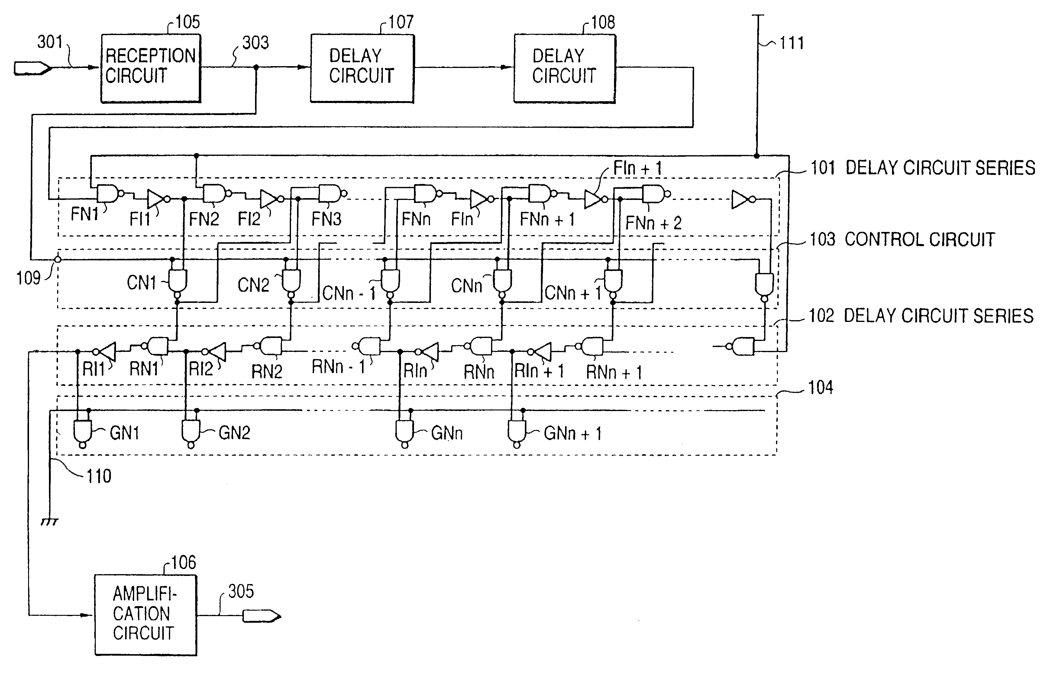
Referring to FIG. 5, the present embodiment is made up of a delay circuit series 101 that can extract output from an arbitrary position of a signal transfer path, a delay circuit series 102 that can input from an arbitrary position of a signal transfer path, a control circuit 103 having a signal input terminal and output terminal and an input / output control terminal 109, a load regulation element 104 for leveling the load of delay circuit series 101 and delay circuit series 102, a reception circuit 105 that receives external signals, an amplification circuit 106, a delay circuit 107 having a delay time equal to reception circuit 105, and a delay circuit 108 having a delay time equal to amplification circuit 106. The output 303 of reception circuit 105 is connected to the input of delay circuit 107 and control terminal 109. The output 303 of delay circuit 107 is connected to the input of delay circui...

second embodiment

The Second Embodiment

The second embodiment of the present invention will next be explained with reference to FIG. 7.

As shown in FIG. 7, this embodiment is configured by adding to the delay circuit device of FIG. 5 a delay circuit 112 that allows selection of a plurality of delay times according to a plurality of control signals, and a delay circuit 113 having equivalent composition delay circuit 112, delay circuit 112 being arranged in a series with the input path of delay circuit series 101, delay circuit 113 being arranged in a series with the output path of delay circuit series 102, and the delay times of delay circuit 112 and delay circuit 113 being controlled so as to be equal.

The operation of this embodiment will next be explained.

The operation of this embodiment is basically equivalent to that of the first embodiment with the difference that the regulation of the delay time dV of delay circuit 112 and delay circuit 113 has been added. Explanation will therefore first be given...

third embodiment

The Third Embodiment

The third embodiment of the present invention will next be explained with reference to FIG. 8.

As shown in FIG. 8, this embodiment involves adding to the delay circuit device of FIG. 5 an inverter 114 that inverts input of amplification circuit 106, the embodiment differing from the first embodiment in that sum of the delay times of delay circuit 107 and delay circuit 108 is set to a time that is shorter than the sum of the delay time of reception circuit 105 and the delay time of amplification circuit 106 by the pulse width of clock 301.

The operation of this embodiment is basically equivalent to that of the first embodiment. However, while an H pulse is inverted to an L pulse when a pulse is transmitted from delay circuit series delay circuit series 102 in the first embodiment, in this embodiment, the L pulse is reinverted to an H pulse and outputted. Because the present embodiment also employs the leading edge of the outputted H pulse, regulation of the pulse wi...


PUM


Abstract

A delay circuit device is described which includes a first delay circuit series that can extract output from any position on a transmission path of a signal, a second delay circuit series that can enter input from any position on a transmission path of a signal, and a control circuit having an input terminal, an output terminal, and an input/output control terminal for signals. The first delay circuit series and the second delay circuit series are arranged such that their signal transmission paths are aligned in opposite directions; the output of the first delay circuit series and the input of the second delay circuit series passing by way of the control circuit and being sequentially connected to each other from the side close to the input of the first delay circuit series and from the side close to the output of the second delay circuit series. A first signal is inputted to the first delay circuit series, a second signal is inputted to the control circuit at an arbitrary subsequent time, and the first signal in the first delay circuit series is transferred to the second delay circuit series.

Description

BACKGROUND OF THE INVENTION1. Field of the InventionThe present invention relates to a semiconductor circuit device, and particularly to a delay circuit device for use in generating transmitting or controlling synchronous signals (hereinafter referred to as "clock pulse").2. Description of the Related ArtAs shown in FIG. 1, a semiconductor circuit device using clock pulses according to the prior art receives an external clock pulse 401 at reception circuit 402, amplifies the clock pulse at an amplification circuit 403, and generates an internal clock pulse 405 for use in circuit 404. As a result, in the process of receiving at reception circuit 402 and amplifying at amplification circuit 403, a delay time 406 is produced between the external clock 401 and the internal clock 402, as shown in FIG. 2. This delay time 406 tends to increase with increased circuit scale of semiconductor circuit devices achieved through progress in manufacturing techniques and the growing diameter of semic...

Claims


Application Information

Patent Timeline
Patent Type & Authority Patents(United States)
IPC IPC(8): H03K5/13H03K5/00H04L7/033H03K5/135G06F1/10G11C11/407G11C11/4076
CPCH03K5/133H03K2005/00071H04L7/0337H03K5/14
Inventor SAEKI, TAKANORI
Owner RENESAS ELECTRONICS CORP
Why Eureka
Try Eureka