Optoelectric composite substrate and method of manufacturing the same

a composite substrate and optoelectric technology, applied in the direction of semiconductor lasers, printed circuit non-printed electric components association, instruments, etc., can solve the problem of not being able to obtain desired optical coupling characteristics, and achieve good optical coupling characteristics and reduce positional discrepancy

Active Publication Date: 2005-09-01
SHINKO ELECTRIC IND CO LTD
View PDF1 Cites 21 Cited by
  • Summary
  • Abstract
  • Description
  • Claims
  • Application Information

AI Technical Summary

Benefits of technology

[0019] It is an object of the present invention to provide an optoelectric composite substrate capable of reducing displacement between an optical device and an optical waveguide in the horizontal direction and capable of setting a distance between the optical device and the optical waveguide to the shortest one, and a method of manufacturing the same.
[0023] Therefore, the optical device can be arranged in close vicinity to the optical waveguide not to touch it and thus the optical coupling characteristics can be improved. Also, since the optical device can be positioned in close vicinity to the optical waveguide, there is not necessary to unnecessarily increase the area of the light incident portion of the optical waveguide. Therefore, the optoelectric composite substrate in the present invention can deal easily with the higher density of the optoelectric composite substrate. In addition, because the distance between the optical device and the optical waveguide can be reduced to the shortest one, the width of the luminous flux can be narrowed when the light is input into the light incident portion of the optical waveguide in the case where the optical device is the light emitting element, for example. Accordingly, since the light from the optical device can be incident on the inner side of the light incident portion of the optical waveguide, a tolerance of the positional discrepancy between the optical device and the light incident portion in the horizontal direction can be set large and thus a positional discrepancy precision in the production process can be relaxed.
[0026] When using such manufacturing method, the optoelectric composite substrate having the foregoing configuration can be easily manufactured. In the present invention, unlike the prior art, the connection terminals are not formed by pasting the substrates together but are formed on the same substrate by a series of productions processes in a state that such connection terminals are aligned with the light incident portion of the optical waveguide with high precision. According to this, the optical device that is mounted on the connection terminals is also mounted in registration with the light incident portion (or the light emission portion) of the optical waveguide.
[0030] As described above, in the optoelectric composite substrate according to the present invention, the optical device can be arranged in close vicinity to the optical waveguide up to the limit and also the positional discrepancy can be reduced. Therefore, the good optical coupling characteristics can be obtained.

Problems solved by technology

Therefore, when the area of the light incident portion A of the optical waveguide 106 is reduced, the luminous flux from the light emitting element 400 is incident on the outside of the light incident portion A. As a result, there exists such a problem that the desired optical coupling characteristics cannot be obtained.

Method used


Image

  • Optoelectric composite substrate and method of manufacturing the same
  • Optoelectric composite substrate and method of manufacturing the same
  • Optoelectric composite substrate and method of manufacturing the same

Examples


first embodiment

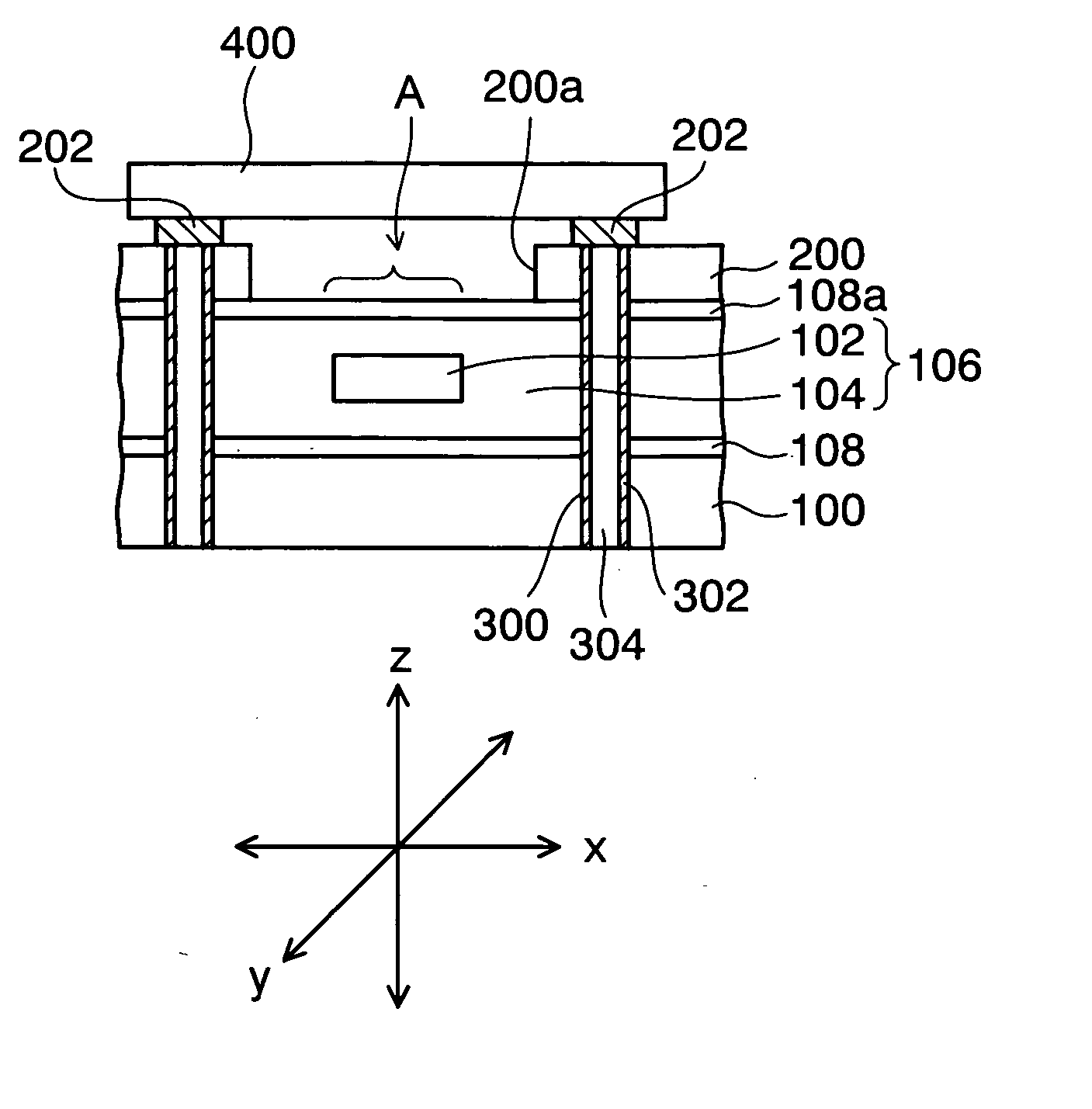
[0048]FIGS. 4A to 4I are sectional views showing a method of manufacturing an optoelectric composite substrate according to a first embodiment of the present invention. FIG. 5 is a partial sectional view showing the situation that an optical device is mounted on the same optoelectric composite substrate.

[0049] In the method of manufacturing the optoelectric composite substrate in the first embodiment of the present invention, as shown in FIG. 4A, first a copper foil 10 acting as a temporal substrate is prepared. Then, as shown in FIG. 4B, an optical waveguide 16 having such a structure that a core portion 14 is surrounded by a cladding portion 12 is formed on one side of the copper foil 10. A refractive index of the core portion 14 is set larger than a refractive index of the cladding portion 12. Where the term “on” used in the manufacturing method in the present embodiment denotes “on the lower surface” in the drawings in some cases.

[0050] As a first example of a method of formin...

second embodiment

[0076]FIGS. 9A to 9I are sectional views showing a method of manufacturing an optoelectric composite substrate according to a second embodiment of the present invention. FIG. 10 is a partial sectional view showing the situation that an optical device is mounted on the same optoelectric composite substrate. The feature of the second embodiment resides in that, since the upper surface of the optical waveguide is formed to project from the upper surface of the insulating film, a distance between the optical device and the optical waveguide is adjusted by a height of the connection terminals and a projection height of the optical waveguide. In FIGS. 9A to 9I, explanation of the same steps as those in the first embodiment will be omitted herein.

[0077] In the method of manufacturing the optoelectric composite substrate in the second embodiment, as shown in FIG. 9A, first the copper foil 10 serving as the temporal substrate is prepared, like the first embodiment. Then, as shown in FIG. 9B...

third embodiment

[0109]FIGS. 13A to 13D are partial sectional views showing a method of manufacturing an optoelectric composite substrate according to a third embodiment of the present invention. FIG. 14 is a partial sectional view showing the situation that the optical device is mounted on the same optoelectric composite substrate.

[0110] A feature of the third embodiment resides in that the connection terminals are embedded in the upper-side portions of the via holes such that their upper surfaces and the upper surface of the insulating film constitute a coplanar surface, and the distance between the optical device and the optical waveguide is adjusted based on a height of bumps provided to the optical device. The same reference symbols are affixed to the same elements as those in the first and second embodiments, and their explanation will be omitted herein.

[0111] In the method of manufacturing the optoelectric composite substrate according to the third embodiment, as shown in FIG. 13A, accordin...


PUM

PropertyMeasurementUnit
widthaaaaaaaaaa
areaaaaaaaaaaa
refractive indexaaaaaaaaaa

Abstract

An optoelectric composite substrate of the present invention includes an insulating film, an optical waveguide embedded in the insulating film in a state that an upper surface is exposed from the insulating film, a via hole formed to pass through the insulating film, a conductor formed in the via hole, and a connection terminal on which an optical device is mounted and which is connected to an upper end side of the conductor, wherein the connection terminal is embedded in an upper-side portion of the via hole or is projected from the insulating film.

Description

CROSS-REFERENCE TO RELATED APPLICATIONS [0001] This application is based on and claims priority of Japanese Patent Application No. 2004-51001 filed on Feb. 26, 2004, the entire contents of which are incorporated herein by reference. BACKGROUND OF THE INVENTION [0002] 1. Field of the Invention [0003] The present invention relates to an optoelectric composite substrate and a method of manufacturing the same and, more particularly, an optoelectric composite substrate constructed to have electric signal wirings and light signal waveguides and a method of manufacturing the same. [0004] 2. Description of the Related Art [0005] Recently it is the electric wirings in the information terminal that are forming a bottleneck while the provision of trunk communication lines is making steadily progress mainly based on the optical fiber communication technology. In order to pass the limit of the transfer rate of the electric signal, the optoelectric composite substrate of the type that the signal ...

Claims


Application Information

Patent Timeline
Patent Type & Authority Applications(United States)
IPC IPC(8): G02B6/122G02B6/12G02B6/43H01L25/16H01S5/00H05K1/02H05K1/11H05K1/18H05K3/40
CPCG02B6/43G02B2006/121H05K2203/0152H05K3/4007H05K3/4644H05K1/0274H01L2224/16225H01L2924/15192
Inventor YONEKURA, HIDEKIKODAIRA, TADASHI
Owner SHINKO ELECTRIC IND CO LTD
Why Eureka
Try Eureka