Flip-chip mounting apparatus

a technology of mounting apparatus and flip-chip, which is applied in the direction of soldering apparatus, mechanical control devices, instruments, etc., can solve the problems of bumps and pads forming, displacement between bumps and pads, and large differences in thermal expansion coefficient between resins of substrate materials

Inactive Publication Date: 2009-04-09
SHINKO ELECTRIC IND CO LTD
View PDF37 Cites 47 Cited by
  • Summary
  • Abstract
  • Description
  • Claims
  • Application Information

AI Technical Summary

Benefits of technology

[0030]According to the present invention, the variable-shape mirror is controlled such that the intensity distribution of the reflected laser beam corresponds to the distribution of the bumps on the semiconductor chip. As a result, the beam shape of the reflected laser beam matches with the outer shape of the semiconductor chip and also the joining portions are heated concentratedly. Therefore, such advantages can be achieved that a temperature of the substrate made of resin seldom rises and also the occurrence of displacements between the bumps and the pads or cracks in the joined portions due to a thermal shrinkage of the resin can be reduced to a minimum.

Problems solved by technology

However, there is a great difference in coefficient of thermal expansion between a resin of the substrate material and a silicon of the semiconductor chip.
Therefore, because of shrinkage of the substrate after the connection is completed, such a problem is caused that either displacements occur between the bumps and the pads or cracks open in the joined portions.
In particular, these days the bumps and the pads are formed in patterns at a narrow pitch due to a high-density wiring demands.
As a result, the problem of above displacements or cracks arises conspicuously.
When the ceramic heater is used, temperature rises slowly and an overshoot is large.
Therefore, temperature control is difficult, which also constitutes one factor of the problem.
As a result, the occurrence of displacements or cracks due to a thermal shrinkage cannot be completely eliminated.

Method used


Image

  • Flip-chip mounting apparatus
  • Flip-chip mounting apparatus
  • Flip-chip mounting apparatus

Examples


Embodiment Construction

[0041]Preferred embodiments of the present invention will be explained in detail with reference to the accompanying drawings hereinafter.

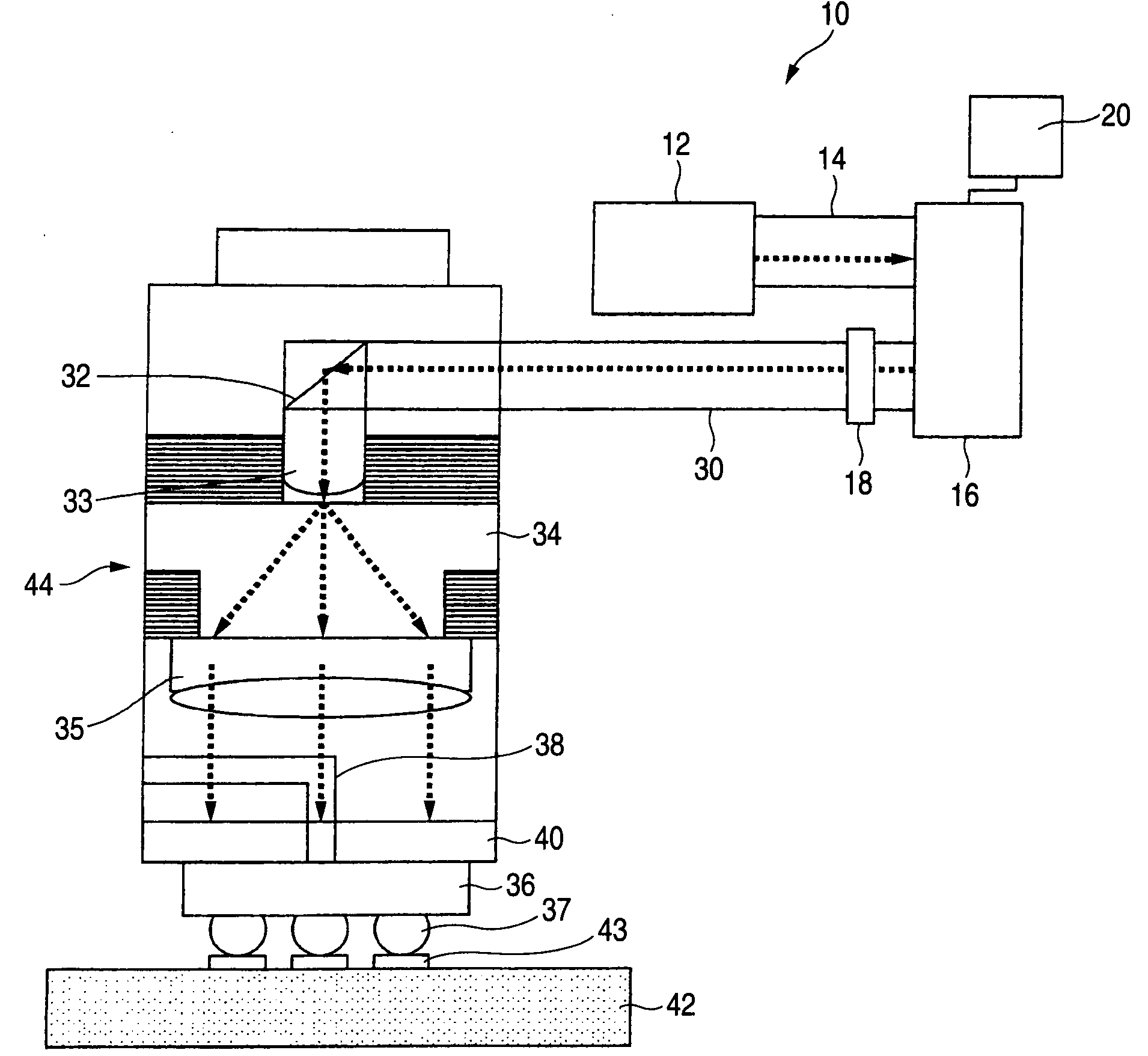
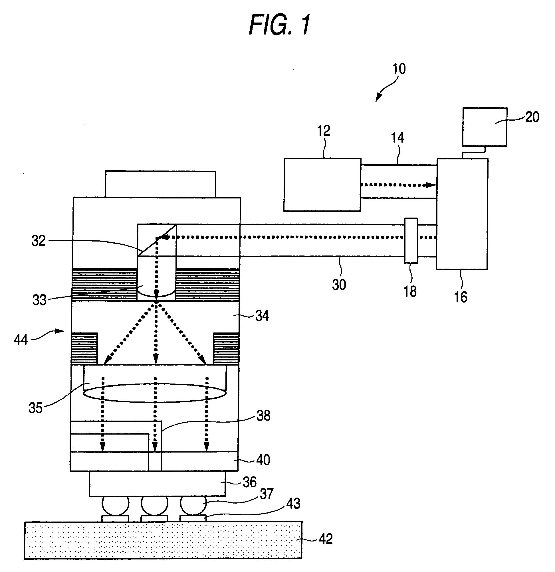
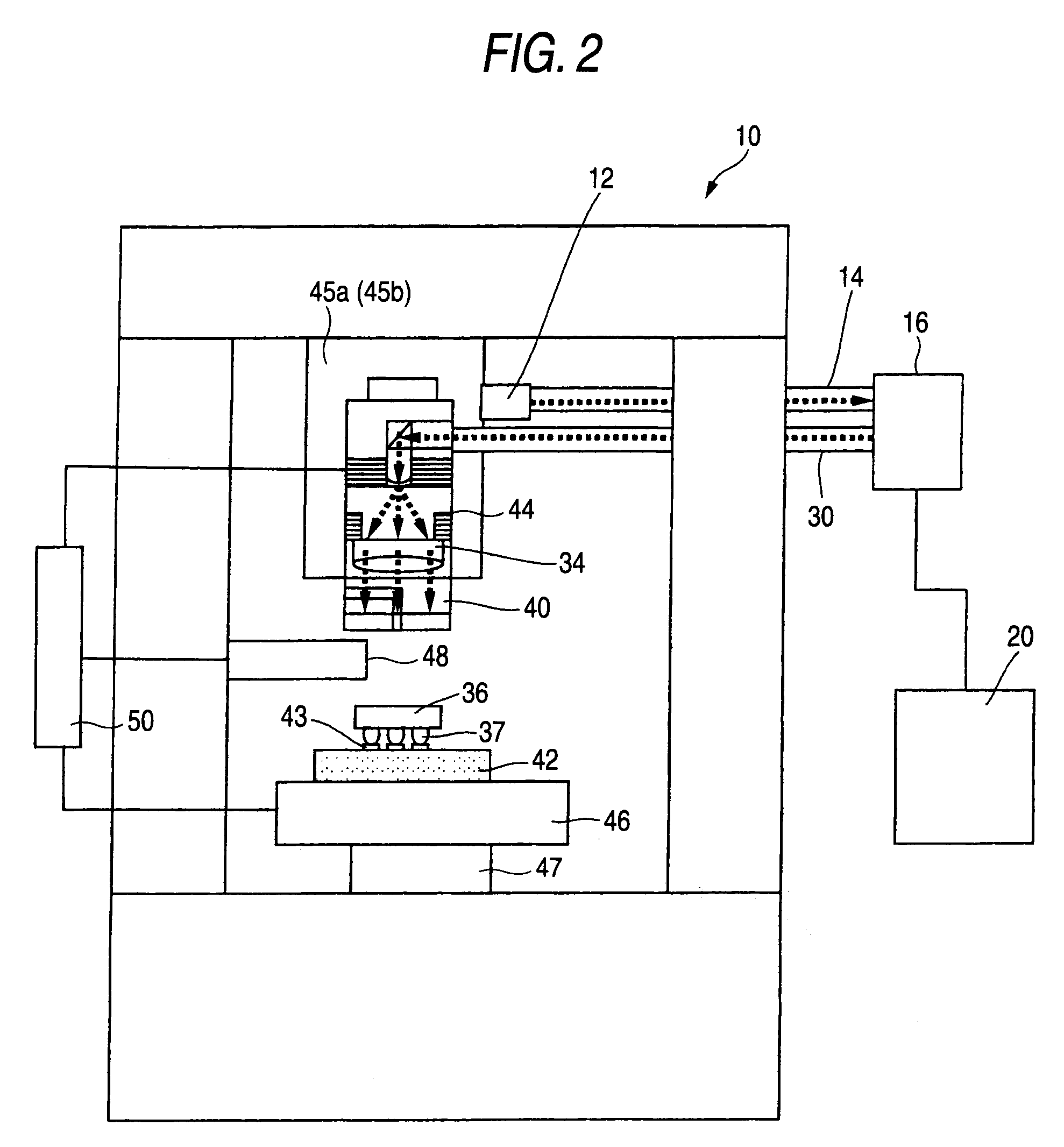
[0042]FIG. 1 is a schematic view of major portions of a flip-chip mounting apparatus 10, and FIG. 2 is a schematic view of an overall flip-chip mounting apparatus.

[0043]A reference numeral 12 denotes a laser beam oscillating source. The laser is not particularly limited; either of a gas laser, a solid laser, a semiconductor laser, and the like may be employed. Any laser may be employed if such laser can heat bumps of a semiconductor chip and pads of a substrate up to temperature at which respective joined portions can be flip-chip connected.

[0044]A laser beam emitted from the laser beam oscillating source 12 is incident on a variable-shape mirror 16 through an optical fiber cable 14.

[0045]The laser beam is reflected by the variable-shape mirror 16, and this reflected laser beam is sensed by a sensor 18. The sensor 18 senses intensity distribution o...


PUM

PropertyMeasurementUnit
temperatureaaaaaaaaaa
diameteraaaaaaaaaa

Abstract

A flip-chip mounting apparatus includes a variable-shape mirror 16 for receiving a laser beam emitted from a laser beam oscillating source 12, a sensor 18 for sensing a reflected laser beam from the variable-shape mirror 16, and a controlling portion 20 for controlling the variable-shape mirror 16 by comparing a sensed signal input from the sensor 18 with previously input threshold values such that an intensity distribution of the reflected laser beam corresponds to a distribution of bumps 37 on a semiconductor chip 36, whereby when the reflected laser beam from the variable-shape mirror 16 is irradiated onto the semiconductor chip 36 through a beam expander 34 and a pushing body 40, a beam shape of the reflected laser beam matches with an outer shape of the semiconductor chip 36 and also joined portions are heated concentratedly.

Description

BACKGROUND OF THE INVENTION[0001]1. Field of the Invention[0002]The present invention relates to a flip-chip mounting apparatus for flip-chip connecting a semiconductor chip to a substrate by laser beam.[0003]2. Description of Related Art[0004]When mounting a semiconductor chip, on which bumps for external connection are formed in a required pattern, on a substrate, the flip-chip (FC) connection is carried out by the flip-chip mounting apparatus in a following manner.[0005]That is, positions of the bumps of the semiconductor chip are adjusted and aligned with pads which are formed on the substrate in a required pattern and the semiconductor chip is loaded on the substrate. Then, a ceramic heater is put on a back surface of the semiconductor chip and the semiconductor chip is heated while applying pressure by the ceramic heater. Thereby, the FC connection is obtained by the melted solders.[0006]However, there is a great difference in coefficient of thermal expansion between a resin o...

Claims


Application Information

Patent Timeline
Patent Type & Authority Applications(United States)
IPC IPC(8): G05G15/00H01L21/60
CPCB23K1/0056H01L2924/01074B23K26/0639B23K26/0643B23K26/0665G02B26/06H01L21/563H01L24/75H01L24/81H01L2224/16H01L2224/75H01L2224/75263H01L2224/757H01L2224/75745H01L2224/81121H01L2224/81224H01L2224/81801H01L2224/83102H01L2224/92125H01L2924/01033H01L2924/01082H01L2924/01005H01L2924/01006B23K26/032B23K26/064H01L2924/12042H01L2224/75753H01L2924/00
Inventor MURAYAMA, KEI
Owner SHINKO ELECTRIC IND CO LTD
Why Eureka
Try Eureka