Silk screen printing technology for printed circuit board

A printed circuit board and screen printing technology, applied in the directions of printed circuit, printed circuit manufacturing, printing, etc., can solve the problems of easy contamination, falling off, and long aging on the surface of the ink, and achieve the effect of reducing the phenomenon of character falling off and shortening the time.

Active Publication Date: 2014-03-26
SHENNAN CIRCUITS
View PDF14 Cites 22 Cited by
  • Summary
  • Abstract
  • Description
  • Claims
  • Application Information

AI Technical Summary

Problems solved by technology

[0004] The purpose of the embodiments of the present invention is to provide a screen printing process for printed circuit boards (PCBs), which aims to solve the ink surface that is easily pol

Method used


Image

  • Silk screen printing technology for printed circuit board

Examples


Embodiment Construction

[0015] In order to make the object, technical solution and advantages of the present invention clearer, the present invention will be further described in detail below in conjunction with the accompanying drawings and embodiments. It should be understood that the specific embodiments described here are only used to explain the present invention, not to limit the present invention.

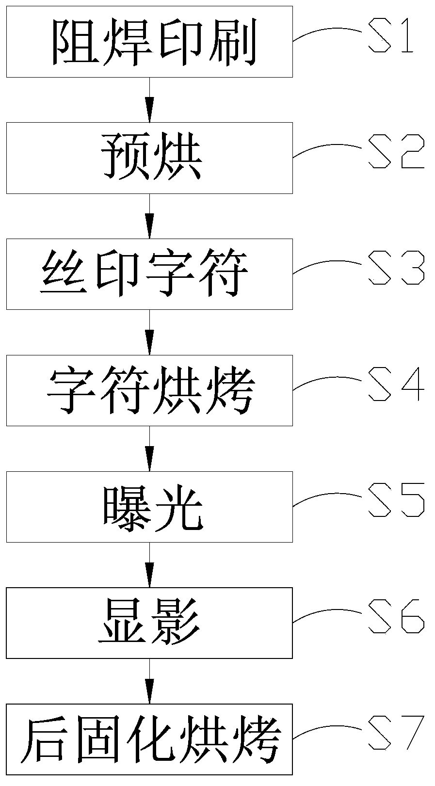
[0016] see figure 1 , the screen printing process for printed circuit board (PCB) provided by the embodiment of the present invention mainly includes the following steps:

[0017] S1) Solder mask printing; specifically, providing a first screen stencil (not shown in the figure), passing the solder resist material through the first screen stencil and printing the pattern on the first screen stencil onto the printed circuit board.

[0018] S2) Pre-baking to drive away the solvent in the solder resist material and partially harden the solder resist material.

[0019] S3) Silk screen characters; spe...


PUM


Abstract

The invention provides a silk screen printing technology for a printed circuit board. The silk screen printing technology for the printed circuit board comprises the steps that a solder mask material is printed on the circuit board after penetrating through a first silk screen template, so that solder mask printing is achieved; pre-drying is conducted so that a solvent in the solder mask material can be removed, and a part of the solder mask material is hardened; a character printing material is printed on the hardened part of the solder mask material after penetrating through a second silk screen template; the character printing material is dried so that a solvent in the character printing material can be removed; exposure is conducted so that sensitization polymerization can occur on a part of the solder mask material; development is conducted so that the part on which sensitization polymerization does not occur of the solder mask material is removed through chemical reaction; post-solidification and post-baking are conducted so that the solder mask material can be hardened thoroughly. According to the silk screen printing technology for the printed circuit board, silk printing of a character is conducted before solder mask exposure, time from solder mask printing to silk printing of the character is greatly shortened, pollution to the surface of printing ink in the exposure process, in the development process and in the post-solidification and post-baking process is avoided, the occurrence rate of the phenomenon of character disengagement caused by poor combination, caused by aging and pollution, between the character and a solder mask layer is reduced.

Description

technical field [0001] The invention belongs to a screen printing process, in particular to a screen printing process for printed circuit boards (PCB). Background technique [0002] Screen printing belongs to stencil printing, and it is called the four major printing methods together with offset printing, embossing printing, and gravure printing. Stencil printing includes stencil printing, perforated printing, inkjet printing and screen printing, etc. The principle of stencil printing is: when the printing plate (the hole that can pass the ink is made on the base of the paper film or other plate), when printing, the ink is transferred to the substrate (paper, ceramics, etc.) ) to form an image or text. Stencil printing is the easiest form of stencil printing. In stencil printing, the most widely used is screen printing. Screen printing is to stretch silk fabrics, synthetic fabrics or wire mesh on the screen frame, and adopts the method of manual engraving paint film or p...

Claims


Application Information

Patent Timeline
IPC IPC(8): B41M1/12H05K3/00
Inventor 刘海龙耿宪国罗斌
Owner SHENNAN CIRCUITS
Why Eureka
Try Eureka