Array substrate and display device
An array substrate and substrate substrate technology, which is applied in the field of array substrates and display devices, can solve problems such as poor display and failure of pixel units to work normally, and achieve the effect of reducing the probability of grid lines or data lines breaking.
- Summary
- Abstract
- Description
- Claims
- Application Information
AI Technical Summary
Problems solved by technology
Method used
Image

Examples
Embodiment Construction
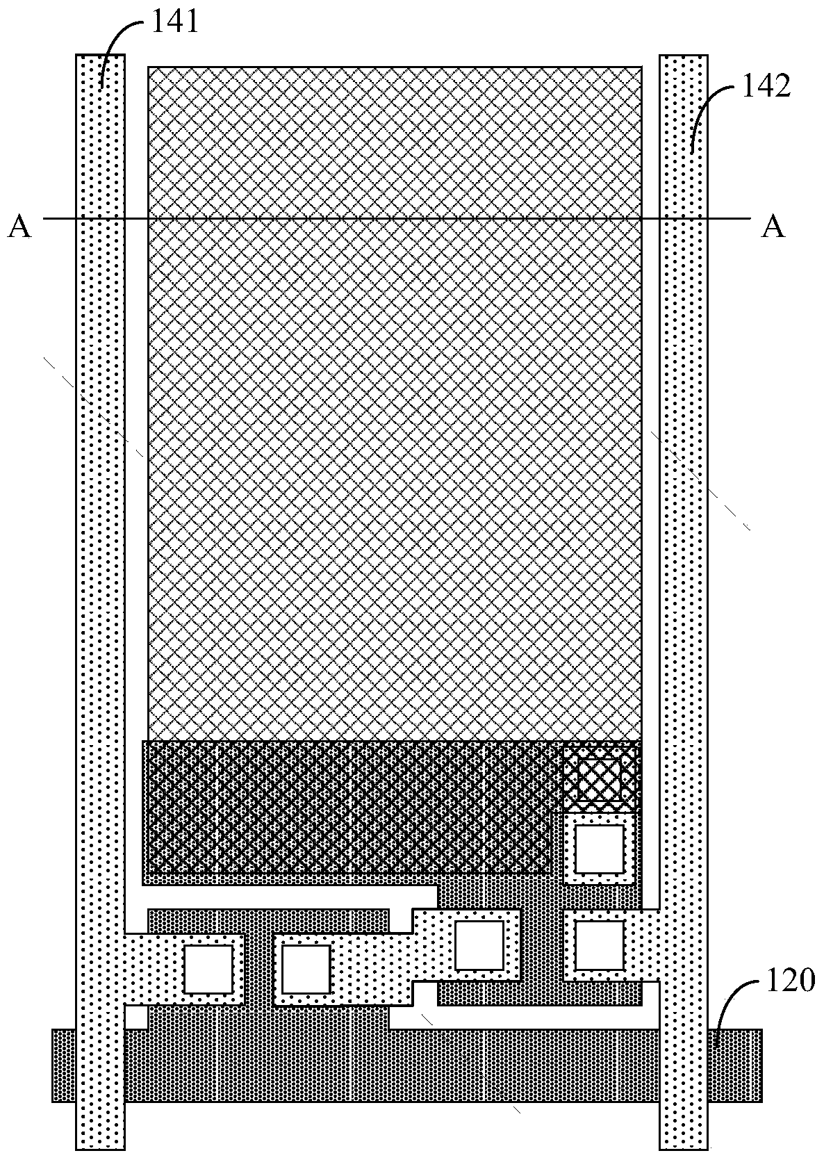
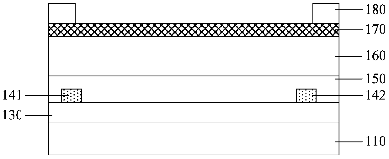
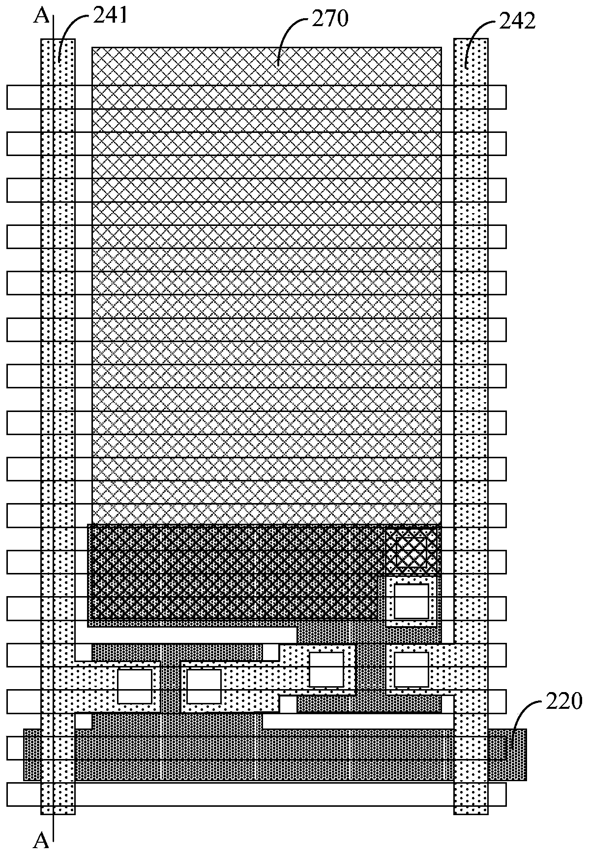
[0028] The array substrate of this embodiment includes structures such as gate lines, gate insulating layers, and data lines formed on the base substrate. gate type TFT) fracture probability, a number of first concave-convex structures are formed on the surface of the gate insulating layer away from the base substrate, so that the gate lines or data lines formed on the gate insulating layer also form a number of first concave-convex structures correspondingly structure, the first concavo-convex structure has the effect of dispersing tension, so that the grid lines or data lines are not easy to break.
[0029] specifically, Figure 2a with 2b As shown, the OLED array substrate is taken as an example, and the thin film transistor is a bottom-gate type, including gate lines 220, gate insulating layer 230, data lines 241, power signal lines 242, and passivation layer 250 formed on the base substrate 210 in sequence. , the resin layer 260 , the anode 270 and the pixel definition ...
PUM
 Abstract
Description
Claims
Application Information
 - R&D
- Intellectual Property
- Life Sciences
- Materials
- Tech Scout
- Unparalleled Data Quality
- Higher Quality Content
- 60% Fewer Hallucinations
Browse by: Latest US Patents, China's latest patents, Technical Efficacy Thesaurus, Application Domain, Technology Topic, Popular Technical Reports.
© 2025 PatSnap. All rights reserved.Legal|Privacy policy|Modern Slavery Act Transparency Statement|Sitemap|About US| Contact US: help@patsnap.com