
PCB thermal pad

A technology for heat dissipation pads and pads, applied in the direction of electrical connection of printed components, printed circuit components, etc., can solve the problems of too fast heat dissipation, pad falling off, and high temperature, so as to reduce rapid heat dissipation and full current flow. , the effect of sufficient heat conduction

Inactive Publication Date: 2014-04-23
SUZHOU HUANYAN ELECTRIC
View PDF5 Cites 5 Cited by
  • Summary
  • Abstract
  • Description
  • Claims
  • Application Information

AI Technical Summary

Problems solved by technology

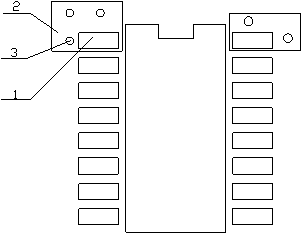
[0004] The technical problem to be solved by the present invention is to provide a PCB heat dissipation pad, which is connected by setting a conductive bridge between each side of the IC power supply and the ground pad and a large area of ​​copper, which solves the problems in the prior art. The pads covering the IC power supply are too fast to dissipate heat and cause high temperature pads to fall off or be damaged during the soldering process

Method used


Image

  • PCB thermal pad
  • PCB thermal pad

Examples


Embodiment Construction

[0020] The technical scheme of the present invention is described in detail below in conjunction with accompanying drawing and embodiment:

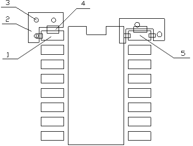
[0021] Such as figure 1 , figure 2 As shown, a PCB heat dissipation pad includes an IC power pad 1, an IC ground pad 5, and a conductive bridge 4. Both the IC power pad 1 and the IC ground pad 5 are square, and the IC power pad At least one side of 1 is connected to the power supply copper skin 2 on the adjacent PCB through a conductive bridge 4, and at least one side of the IC ground pad 5 is connected to the ground copper skin on the adjacent PCB through a conductive bridge 4 , at least one via hole 3 is provided on both the power supply copper skin 2 and the ground copper skin.

[0022] A conductive bridge is set between the ground pad of the IC power supply and the copper skin. In the case of sufficient power supply, the heat loss added to the pad is slowed down, and the damage to the pad caused by heating the pad for a long time d...


PUM


Abstract

The invention discloses a PCB thermal pad which comprises an IC power pad, an IC land pad and conductivity bridges. The IC power pad and the IC land pad are both square. At least one side of the IC power pad is connected with a power copper sheet on an adjacent PCB through the conductivity bridge. At least one side of the IC land pad is connected with a land copper sheet on an adjacent PCB through a conductivity bridge. The power copper sheet and the land copper sheet are both provided with at least a through hole. As the conductivity bridges are arranged between the IC power / land pads and the copper sheets, on the circumstance of full power supply, heat loss of the pads is slowed down. As heat loss is too fast, the pads will be damaged if heated for a long time. By the adoption of the PCB thermal pad, the above problem will be avoided. In addition, yield of products is increased and reliable performance is raised.

Description

technical field [0001] The invention discloses a PCB cooling pad, which is used for connecting the power supply and the ground pad of an IC on a circuit board with the surrounding large-area copper covering, and belongs to the field of PCBs. Background technique [0002] At present, in the design of some high-power PCB boards, heat dissipation is the most concerned issue. In the process of PCB wiring, it is necessary to consider not only the size of the current, but also the heat dissipation problem, and also the radiation problem. Therefore, , In PCB wiring, the reasonable layout of the power ground largely determines the quality of the product. The heat dissipation of the power ground on the PCB generally adopts the method of covering a large area with copper, so that the heat can be dissipated quickly, and at the same time, the large area of ​​copper can be Make sure enough current flows through. In order to facilitate wiring, the wiring personnel use large-area copper p...

Claims


Application Information

Patent Timeline
Patent Type & Authority Applications(China)
IPC IPC(8): H05K1/02H05K1/11
Inventor 颜欢
Owner SUZHOU HUANYAN ELECTRIC
Learn More