Flash memory and bad block managing method thereof

A flash memory and storage module technology, applied in the field of NAND Flash memory, can solve the problems of poor reliability, high cost and application complexity of NAND Flash memory cells, inability to realize SPINAND products, etc., to improve system reliability, reduce responsibility, The effect of solving bottlenecks

Active Publication Date: 2014-05-07
GIGADEVICE SEMICON (BEIJING) INC
View PDF5 Cites 26 Cited by
  • Summary
  • Abstract
  • Description
  • Claims
  • Application Information

AI Technical Summary

Problems solved by technology

[0003] It can be seen from the above that in the traditional NAND Flash bad block management scheme, the cost and application complexity are increased due to the use of the driver
More importantly, with the continuous improvement of NAND Flash process nodes, the reliability of NAND Flash storage cells is getting worse and worse, and the simple external bad block management method can no longer meet the demand
In addition, the main control system of the emerging device type SPI NAND Flash usually cannot provide a driver for bad block management (BBM), so such a traditional method cannot realize SPI NAND products

Method used


Image

  • Flash memory and bad block managing method thereof
  • Flash memory and bad block managing method thereof
  • Flash memory and bad block managing method thereof

Examples


Embodiment 1

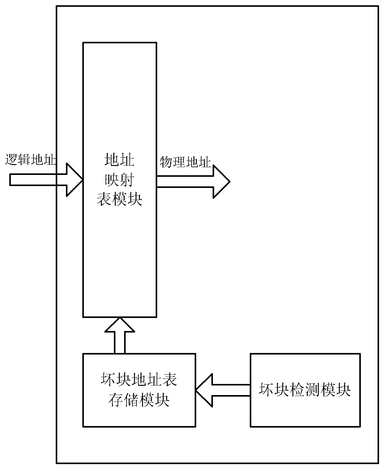
[0030] The present embodiment provides a kind of NAND Flash memory, can realize bad block management inside it, this memory such as figure 2 As shown, it at least includes a block address mapping module, a bad block address table storage module and a bad block detection module.

[0031] The bad block detection module detects the block address corresponding to the access operation initiated by the user, and judges whether the block is a bad block;

[0032] Specifically, the bad block detection module can be realized by using finite state and FSM, that is, to detect the operated block at an appropriate time to judge whether it is a bad block or a good block. The appropriate time can be during the block erase process, or during the operation process of the block program. Generally, the block erase process takes a long time. During this process, all address spaces in this block will be operated. Therefore, once an erase fail cell (storage cell that has failed to be erased) is de...

Embodiment 2

[0040] This embodiment provides a method for managing bad blocks in a flash memory, including:

[0041] Detect the block address corresponding to the access operation initiated by the user, and when the detection determines that a block is a bad block, store the block address of the bad block;

[0042] When receiving the access operation initiated by the user, if the block address in the logical address corresponding to the access operation is found to be the block address of the bad block from the stored block address of the bad block, then the logical address corresponding to the access operation will be The block address of the block is mapped to the block address of the good block, and then the address is decoded.

[0043] Wherein, the flash memory may use a non-volatile storage unit to store the block address of the bad block.

[0044] During the implementation of the above method, the flash memory can detect whether there is a storage cell that fails to be erased in the b...


PUM


Abstract

The invention discloses a flash memory and a bad block managing method of the flash memory, and relates to the technical field of NANDFlash memories. The flash memory comprises a bad block detection module, a bad block address table memory module and a block address mapping module. The bad block detection module detects a block address corresponding to access operation initiated by a user and judges whether a block is a bad block or not, the bad block address table memory module conducts memory on the block address of the bad block judged by the bad block detection module, when the block address mapping module receives the access operation initiated by the user, the block address mapping module inquires whether the block address, corresponding to the access operation, in the logic address is the block address of the bad block or not from the bad block address table memory module, and if the block address, corresponding to the access operation, in the logic address is the block address of the bad block, the block address, corresponding to the access operation, in the logic address is mapped to the block address of a good block, and then is sent into the flash memory to conduct address decoding. The invention further discloses a bad block managing method by the flash memory. According to the technical scheme, the reliability of the system is improved, and the bottleneck of a SPI NAND Flash application is overcome.

Description

technical field [0001] The invention relates to the technical field of NAND Flash memory, in particular to a NAND Flash chip and a method for managing bad blocks thereof. Background technique [0002] Compared with NOR Flash, the existing NAND Flash has not only defects in the manufacturing process, but also defects in the use process, especially in large-capacity chips, this mechanism is inevitable. Therefore, traditional NAND Flash requires a responsible driver to help the system manage NAND, and the management of bad blocks is essential. In the process of using traditional NAND Flash, the external driver serves as the interface between the main control and NAND Flash to manage the bad block mechanism and other aspects, such as figure 1 shown. [0003] It can be seen from the above that in the traditional NAND Flash bad block management scheme, the cost and application complexity are increased due to the use of the driver. More importantly, with the continuous improveme...

Claims


Application Information

Patent Timeline
Patent Type & Authority Applications(China)
IPC IPC(8): G06F12/02
Inventor 苏志强张现聚刘奎伟丁冲
Owner GIGADEVICE SEMICON (BEIJING) INC
Why Eureka
Try Eureka