goi_tddb test circuit structure

A technology for testing circuits and gate oxide layers, which is applied to circuits, electrical components, and electric solid-state devices, etc. It can solve the problems of reducing the performance of gate oxide layer 2, increasing defects, and destroying GOI_TDDB test results, etc., so as to achieve reliable test results and complete protection sexual effect

Active Publication Date: 2016-10-05
SEMICON MFG INT (SHANGHAI) CORP
View PDF6 Cites 0 Cited by
  • Summary
  • Abstract
  • Description
  • Claims
  • Application Information

AI Technical Summary

Problems solved by technology

When the conductive channel width (critical dimension) drops below 65nm, the squeeze effect of the STI 6 outside the source region 41 and the drain region 42 on the MOS structure cannot be ignored, and it will squeeze the gate oxide layer 2 therein. In turn, the defects of the gate oxide layer 2 increase, thereby reducing the performance of the gate oxide layer 2, thereby destroying the GOI_TDDB test results, so that the GOI_TDDB test results cannot reflect the real device performance

Method used


Image

  • goi_tddb test circuit structure
  • goi_tddb test circuit structure
  • goi_tddb test circuit structure

Examples


Embodiment Construction

[0035] In order to make the purpose, technical solution and advantages of the present invention more clear, the present invention will be further described in detail below with reference to the accompanying drawings and examples.

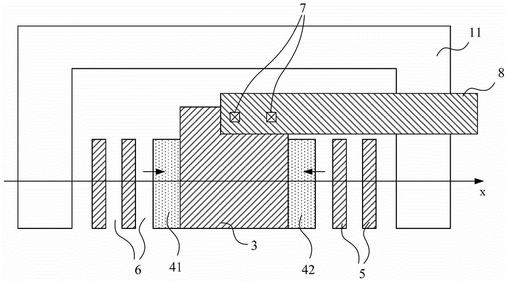
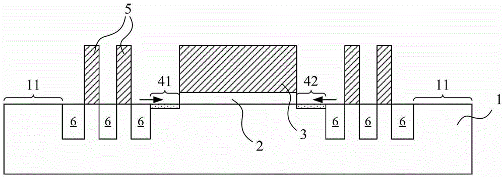
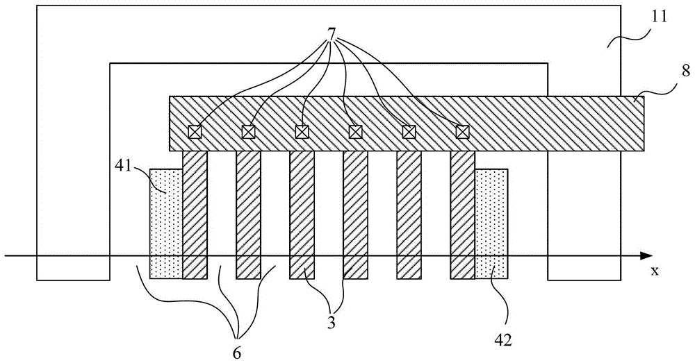
[0036] like Figure 2a , Figure 2b As shown, the GOI_TDDB test circuit of the present invention includes a substrate 1 , a gate oxide layer 2 , a polysilicon layer 3 , a source region 41 , a drain region 42 and an STI 6 .

[0037] Wherein, the gate oxide layer 2 is formed on the substrate 1, and there are multiple gate oxide layers 2, and the gate oxide layers 2 are parallel to each other and distributed in a finger shape; wherein, the substrate 1 can be an N-type substrate bottom or P-type substrate. The polysilicon layer 3 is deposited on the gate oxide layer 2, and the distribution of the gate oxide layer 2 is the same. A polysilicon layer 3 is deposited one to the other. An STI 6 is formed in the substrate 1 between adjacent gate oxide laye...


PUM


Abstract

The invention discloses a GOI_TDDB test circuit structure comprising a substrate, a plurality of gate oxide layers which are formed on the substrate, are parallel to each other and are in finger-shaped distribution, polysilicon layers which are deposited on the gate oxide layers, are parallel to each other and are in finger-shaped distribution, source and drain electrode regions which are at outer substrates which are at outermost gate oxide layers and are far from other gate oxide layers, and STIs which are formed in the substrate, are between gate oxide layers and are at the outer sides of the gate oxide layers and the source and drain electrode regions. According to the GOI_TDDB test circuit structure, since the gate oxide layers which are parallel to each other and are in finger-shaped distribution and the polysilicon layers which are parallel to each other and are in finger-shaped distribution are employed, the STIs are added between adjacent gate oxide layers, the source and drain electrode regions with width larger than or equal to 1.3 micrometers are employed, when the width of a conductive channel is less than 65 nanometers, the appearance of the gate oxide layers in the GOI_TDDB test circuit structure can be effectively protected, and thus the result of a GOI_TDDB test is accurate and reliable.

Description

technical field [0001] The present invention relates to the field of semiconductor testing, in particular to a GOI_TDDB (Gate OxideIntegrity_Time Dependent Dielectric Breakdown, Gate Oxide Integrity_Time Dependent Dielectric Breakdown) testing circuit structure for semiconductors. Background technique [0002] The GOI_TDDB (Gate Oxide Integrity_Time Dependent Dielectric Breakdown) test of semiconductors is a very important test item in semiconductor testing. It can be used to predict the service life of semiconductor devices. [0003] The gate structure of a MOS (Metal Oxide Semiconductor) device consists of a gate oxide layer formed on the substrate and a polysilicon layer deposited on the gate oxide layer, where the substrate material is a silicon substrate, the gate oxide layer The material is silicon dioxide. The leakage current of the gate oxide layer has a great relationship with the quality of the gate oxide layer, and the leakage point increases to a certain extent...

Claims


Application Information

Patent Timeline
Patent Type & Authority Patents(China)
IPC IPC(8): H01L23/544
Inventor 牛刚刘竞文于建姝赵晓东段晓博
Owner SEMICON MFG INT (SHANGHAI) CORP
Why Eureka
Try Eureka