Method for measuring external parasitic resistance of MOS transistor

A MOS transistor and parasitic resistance technology, which is applied in the field of external parasitic resistance measurement, can solve problems such as complex methods, achieve simple methods and processes, improve measurement efficiency, and achieve uniform changes.

Active Publication Date: 2014-06-04
SEMICON MFG INT (SHANGHAI) CORP
View PDF9 Cites 14 Cited by
  • Summary
  • Abstract
  • Description
  • Claims
  • Application Information

AI Technical Summary

Problems solved by technology

[0007] However, the above method of measuring the external parasitic resistance of the transistor is more complicated

Method used


Image

  • Method for measuring external parasitic resistance of MOS transistor
  • Method for measuring external parasitic resistance of MOS transistor
  • Method for measuring external parasitic resistance of MOS transistor

Examples


Embodiment Construction

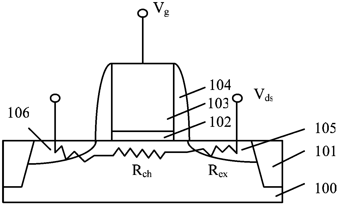
[0030] At present, when measuring the external parasitic resistance of transistors, at least three transistors need to be formed on the semiconductor substrate. The formation process of the three transistors is the same, and the lengths of the channel regions are different, and then the gates of the three transistors are respectively applied to work. Voltage and source apply a small source voltage to make the three transistors work in the linear region, and then perform a straight line fitting according to the obtained three source-drain resistances of the three transistors and the corresponding channel region lengths to obtain the external For parasitic resistance, the inventors found that this measurement method is relatively complicated and has low efficiency.

[0031] For this reason, the inventor proposes a method for measuring the external parasitic resistance of a MOS transistor, including: providing a semiconductor substrate, forming a MOS transistor on the semiconducto...


PUM


Abstract

A method for measuring the external parasitic resistance of an MOS transistor comprises the steps that a semiconductor substrate is provided, and the MOS transistor is formed on the semiconductor substrate; a first voltage is applied to the gate electrode of the MOS transistor, a second voltage is applied to the source electrode of the MOS transistor, the first voltage is increased gradually, the second voltage remains unchanged, and at least ten source leakage current values corresponding to different first voltage values are obtained through measurement; according to the second voltage and the source leakage current values, at least ten MOS transistor source leakage resistance values corresponding to the different first voltage values are obtained through calculation, wherein the MOS transistor source leakage resistance comprises channel region resistance and the external parasitic resistance; curve fitting is conducted on the different first voltage values and the corresponding MOS transistor source leakage resistance values for five times, so that the external parasitic resistance of the MOS transistor is obtained. According to the method for measuring the external parasitic resistance of the MOS transistor, the measuring process is simple and convenient.

Description

technical field [0001] The invention relates to the field of semiconductor manufacturing, in particular to a method for measuring the external parasitic resistance of a MOS transistor. Background technique [0002] In the existing integrated circuit manufacturing, with the continuous advancement of semiconductor integrated circuit technology and the continuous reduction of feature size, the number of devices on a single wafer has continued to increase, the function of the circuit has been improved, the circuit has become increasingly complex, and the process The links in manufacturing are required to be more and more refined, and the reliability of devices is becoming more and more important. [0003] Metal-oxide-semiconductor (MOS) transistors are the most basic devices in semiconductor manufacturing. They are widely used in various integrated circuits. According to the main carrier and the type of doping during manufacturing, they are divided into NMOS and PMOS transistors...

Claims


Application Information

Patent Timeline
Patent Type & Authority Applications(China)
IPC IPC(8): G01R27/14
Inventor 陈乐乐
Owner SEMICON MFG INT (SHANGHAI) CORP
Why Eureka
Try Eureka