Method and device for writing data in memory chip

A data writing and storage chip technology, applied in the embedded field, can solve the problems of loss of storage/reading function, data inaccessibility, storage unit damage, etc., to reduce the probability of data loss and reduce the cost of writing and erasing The number of times, the effect of prolonging the working life

Active Publication Date: 2014-06-04
GUANGZHOU HUAXIN ELECTRONICS TECH
View PDF4 Cites 6 Cited by
  • Summary
  • Abstract
  • Description
  • Claims
  • Application Information

AI Technical Summary

Problems solved by technology

[0003] However, during the rewriting process of today's Flash memory chips, the number of erase operations and write operations is limited, such as figure 1 As shown, when a certain system or in a certain use environment needs to frequently modify a certain parameter in the Flash memory chip, due to the particularity of the Flash memory chip, the page erase action is performed when erasing, so when it is necessary to modify the figure 1 When rewriting C3 data, when C3 is written 100K times, P1 page is correspondingly erased 100K times. However, other parameters alway

Method used


Image

  • Method and device for writing data in memory chip
  • Method and device for writing data in memory chip
  • Method and device for writing data in memory chip

Examples


Example Embodiment

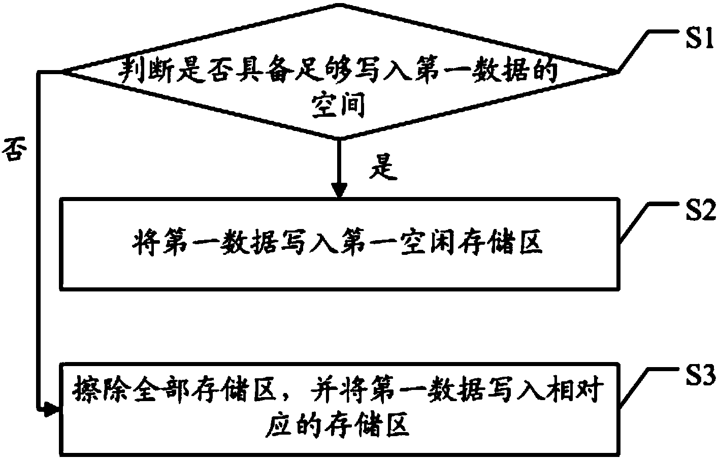
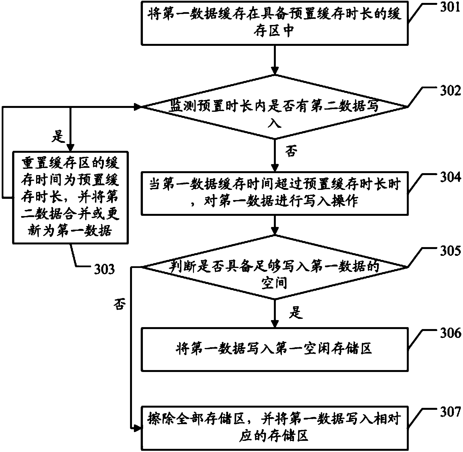
[0057] The embodiment of the present invention provides a method and device for writing data to a memory chip, which first determines whether there is enough space for writing new data, if so, writes the new data directly, if not, then performs an erase operation Therefore, the number of times of writing and erasing in the Flash memory chip is further reduced, and at the same time, the working life of the Flash memory chip is greatly extended.

[0058] In order to make the objectives, features, and advantages of the present invention more obvious and understandable, the technical solutions in the embodiments of the present invention will be described clearly and completely with reference to the accompanying drawings in the embodiments of the present invention. Obviously, the following The described embodiments are only a part of the embodiments of the present invention, rather than all the embodiments. Based on the embodiments of the present invention, all other embodiments obtai...


PUM


Abstract

The embodiment of the invention discloses a method and device for writing data in a memory chip. According to the method and device, whether enough space for writing of new data exists or not is judged, if yes, the new data are directly written in, and if not, an erasing operation is carried out. Therefore, the frequency of writing operations and the frequency of erasing operations in the Flash memory chip are further reduced, and the service life of the Flash memory chip is greatly prolonged. The method comprises the steps of (1) judging whether enough space for writing of first data exists or not , if yes, executing the step (2), if not, executing the step (3), (2) writing the first data in a first idle memory area, and (3) erasing all the memory areas, and writing the first data in the corresponding memory area.

Description

technical field [0001] The invention relates to the field of embedded technology, in particular to a method and device for writing data into a memory chip. Background technique [0002] Flash storage chip is the specific application of the concept of embedded system chips in the storage industry. The most important storage chips in embedded system chips are Flash storage chips and RAM chips. However, because the data of Flash storage chips will not The lost special function makes the application of Flash memory chip more extensive. [0003] However, during the rewriting process of today's Flash memory chips, the number of erase operations and write operations is limited, such as figure 1 As shown, when a certain system or in a certain use environment needs to frequently modify a certain parameter in the Flash memory chip, due to the particularity of the Flash memory chip, the page erase action is performed when erasing, so when it is necessary to modify the figure 1 When r...

Claims


Application Information

Patent Timeline
IPC IPC(8): G06F3/06
Inventor 邓孜俊王龙辉左春生刘伟高
Owner GUANGZHOU HUAXIN ELECTRONICS TECH
Why Eureka
Try Eureka