Manufacturing method of mold for nanoimprinting

A technology of nano-imprinting and manufacturing method, which is applied in the directions of nanotechnology, nanotechnology, nanotechnology for information processing, etc., can solve the problem of increasing the probability of damage to the main mold, making it difficult to form the conductive seed layer 14, and reducing the mechanical properties of the mold. Durability and other issues, to improve durability and reliability, reduce production costs, and improve efficiency

Inactive Publication Date: 2017-03-22
LG INNOTEK CO LTD
View PDF2 Cites 2 Cited by
  • Summary
  • Abstract
  • Description
  • Claims
  • Application Information

AI Technical Summary

Problems solved by technology

However, there is a problem in the mold manufacturing method using electroforming that it is difficult to form the conductive seed layer 14, and holes 16 are formed inside the mold during the electroforming process, reducing the mechanical properties and durability of the mold, and increasing the Chance of breakage of master mold during separation of manufactured mold from grid pattern 13

Method used


Image

  • Manufacturing method of mold for nanoimprinting
  • Manufacturing method of mold for nanoimprinting
  • Manufacturing method of mold for nanoimprinting

Examples


Embodiment Construction

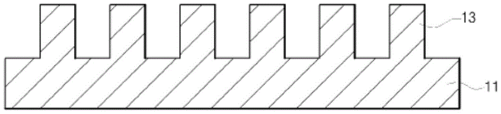
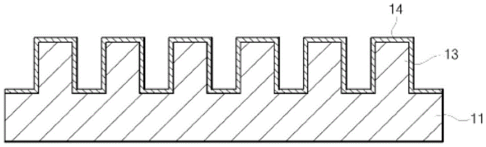
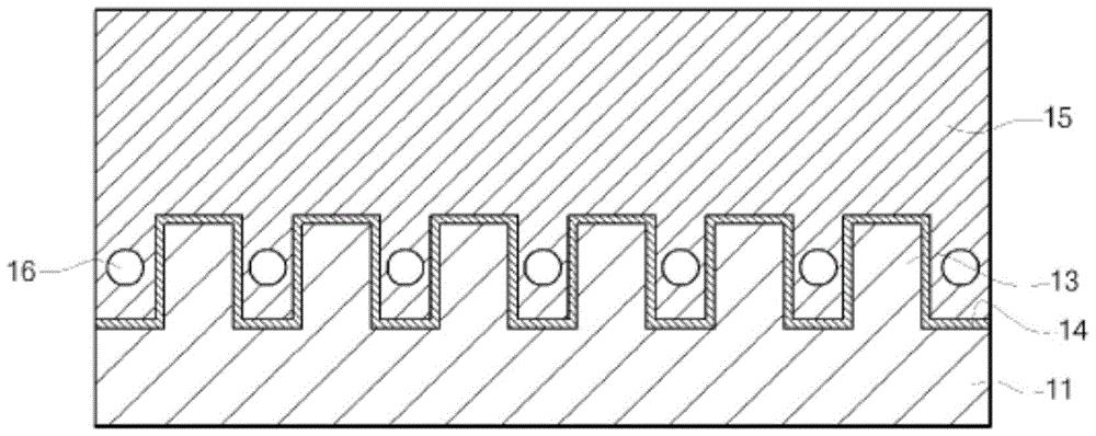
[0030] Exemplary embodiments according to the present invention will be described more fully below with reference to the accompanying drawings so that those of ordinary skill in the art to which the present invention pertains can easily implement the exemplary embodiments of the present invention. The exemplary embodiment described herein and the elements illustrated in the drawings are only one preferred exemplary embodiment of the present invention. It should be understood that there are various equivalents and modifications that may be substituted for these embodiments and elements at the time of filing this application. Also, when referring to detailed descriptions of the operating principles of the preferred exemplary embodiments, when considering that detailed descriptions about well-known functions or elements may unnecessarily obscure the gist of the exemplary embodiments of the present invention, they are omitted. These are detailed. Terms to be described below are t...


PUM

PropertyMeasurementUnit
widthaaaaaaaaaa

Abstract

Provided is a method of manufacturing a mold for nano imprint comprising: forming a plurality of grid patterns on a substrate; forming a metal grid pattern on the grid patterns; forming a plated layer on the metal grid pattern; and separating a mold consisting of the metal grid pattern and the plated layer from the grid pattern, which can reduce a production cost, improve the efficiency of a process, and provide the mold for nano having improved durability and reliability.

Description

[0001] Cross References to Related Applications [0002] This application claims priority from Korean Patent Application No. 10-2011-0075191 filed with the Korean Intellectual Property Office on Jul. 28, 2011, the entire contents of which are hereby incorporated by reference. technical field [0003] Exemplary embodiments of the present invention relate to the technical field of manufacturing a mold for nanoimprinting. Background technique [0004] A polarizer or polarizing device refers to an optical device that extracts linearly polarized light having a specific vibration direction out of unpolarized light such as natural light. In general, in the case where the arrangement period of metal wires is less than half the wavelength of incident electromagnetic waves, a polarization component (s-wave) parallel to the metal wires is reflected and a polarization component (p-wave) perpendicular to the metal wires is transmitted. Using this phenomenon, planar polarizers with excel...

Claims


Application Information

Patent Timeline
Patent Type & Authority Patents(China)
IPC IPC(8): G02B5/30
CPCB23P15/24B29C33/424B29D11/00346B29D11/0048B29D11/00644B81C99/009B82Y10/00B82Y40/00C25D1/006C25D1/10C25D1/20C25D5/022G02B5/3058G03F7/0002
Inventor 刘庆钟李领宰金镇秀李俊
Owner LG INNOTEK CO LTD
Why Eureka
Try Eureka