Method for preparing dual-period nanostructure through laser interference nanolithography
A nano-lithography and laser interference technology, which is applied in the expansion field of laser interference nano-lithography technology in the manufacture of single-cycle nanostructures, can solve the problems of uneven imprinting and extremely high surface roughness requirements, and achieve high processing efficiency , flexible and diverse manufacturing methods, and low manufacturing costs
- Summary
- Abstract
- Description
- Claims
- Application Information
AI Technical Summary
Problems solved by technology
Method used
Image
Examples
Embodiment 1
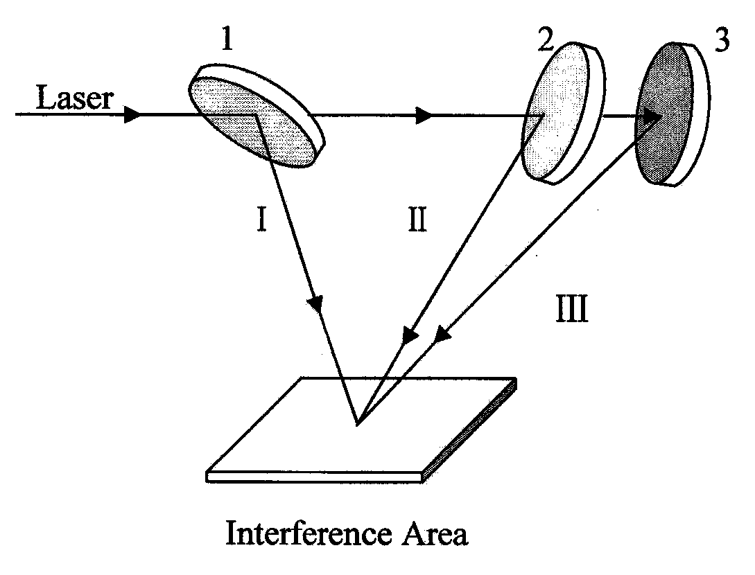
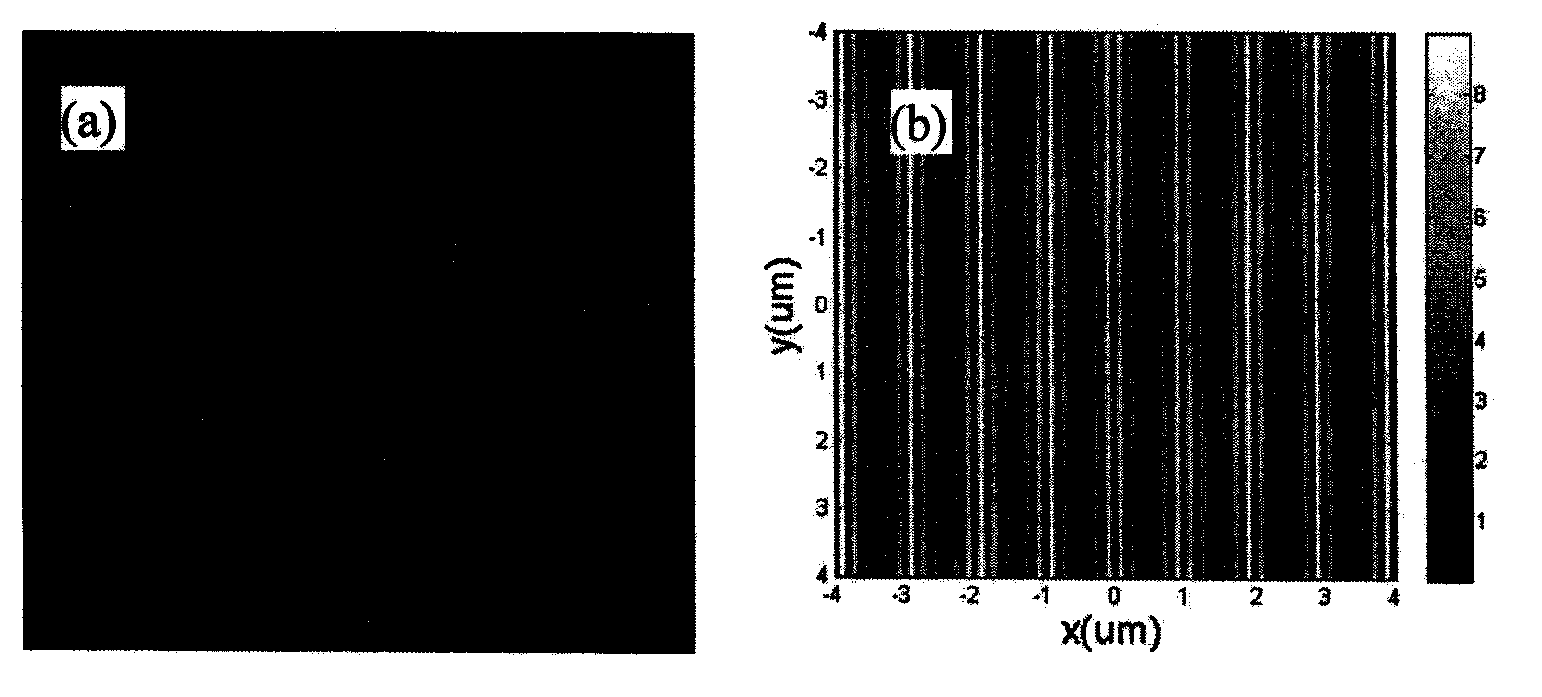
[0027] like figure 2 As shown, the laser is emitted by a He-Ne laser (633nm), and the beam is divided into three beams of coherent light by the beam splitter 1 and 2 and the high reflection mirror 3. In the figure, optical paths I and II are incident light beams, and optical path III is a modulated light beam. The spatial angles of the incident light I and II are distributed symmetrically to the central axis of the system, that is, 0° and 180°, and the spatial angle of the modulated light III is the same as that of any of the two incident light beams, but the incident angles are different. The incident angle of the incident beam is 6°, and the incident angle of the modulated beam is 9°. The light intensity and polarization angle of each beam are precisely controlled by wave plates and polarization devices, and a double structure under specific conditions is formed in the interference field. image 3 It is the interference structure diagram and matlab simulation diagram of E...
Embodiment 2
[0029] like Figure 4 As shown, the laser light sent by the He-Ne laser (633nm) passes through the beam splitter 1 and reaches the interference field as the optical path I; through the beam splitters 1, 2 and 3 and reaches the interference field as the optical path II; through the beam splitters 1, 2 and 3, the high Reflector 5 reaches the interference field as optical path III; after passing through beam splitters 1, 2 and 3, high reflection mirror 4 reaches the interference field as optical path IV. In the figure, optical paths I, II, and III are incident light beams, and optical path IV is a modulated light beam. The spatial angles of incident light I, II, and III are symmetrically distributed in the central axis of the system, that is, 0°, 120° and 240°, and the spatial angle of modulated light IV is the same as that of any of the three incident light beams, but the incident angles are different . The incident angle of the incident beam is 6°, and the incident angle of t...
Embodiment 3
[0031] like Image 6 As shown, the laser light emitted by the He-Ne laser (633nm) passes through 1 and reaches the interference field as the optical path I; passes through the beam splitters 1, 2, 3 and 4 and reaches the interference field as the optical path II; passes through the beam splitters 1, 2, 3 and 5 Reaching the interference field is the optical path III; passing through the beam splitters 1 and 2, the high reflective mirrors 6 and 7 reaching the interference field is the optical path IV; passing through the beam splitters 1, 2, 3 and 4, the high reflecting mirror 8 reaching the interference field is the optical path V; passing through Beam splitters 1, 2, 3 and 5, and highly reflective mirrors 9 and 10 reach the interference field as the optical path VI. In the figure, optical paths I, II, and III are incident light beams, and optical paths IV, V, and VI are modulated light beams. The spatial angles of the incident light I, II, and III are symmetrically distribute...
PUM
 Abstract
Description
Claims
Application Information


