Rinse tank for rinsing semiconductor wafer

A technology for cleaning tanks and semiconductors, applied in the field of cleaning tanks, which can solve problems such as incomplete cleaning of 800 particles on a wafer, etc., and achieve the effects of strong cleaning ability, wide cleaning surface, and increased output

Active Publication Date: 2014-06-18
SHANGHAI HUALI MICROELECTRONICS CORP
View PDF4 Cites 19 Cited by
  • Summary
  • Abstract
  • Description
  • Claims
  • Application Information

AI Technical Summary

Problems solved by technology

However, for wafers 800 with complex surface patterns, since the spray pipe 700 cleans the wafers 800 in the fixed position and direction of the cleaning tank, it is easy to cause some particles on the surface of the wafers 800 to be stuck in the patterns and cannot be washed out or the cleaning is not thorough.

Method used


Image

  • Rinse tank for rinsing semiconductor wafer
  • Rinse tank for rinsing semiconductor wafer
  • Rinse tank for rinsing semiconductor wafer

Examples


Embodiment Construction

[0022] The implementation of the present invention will be described in detail below in conjunction with the drawings and examples, so that the realization process of how to use technical means to solve technical problems and achieve technical effects in the present invention can be fully understood and implemented accordingly.

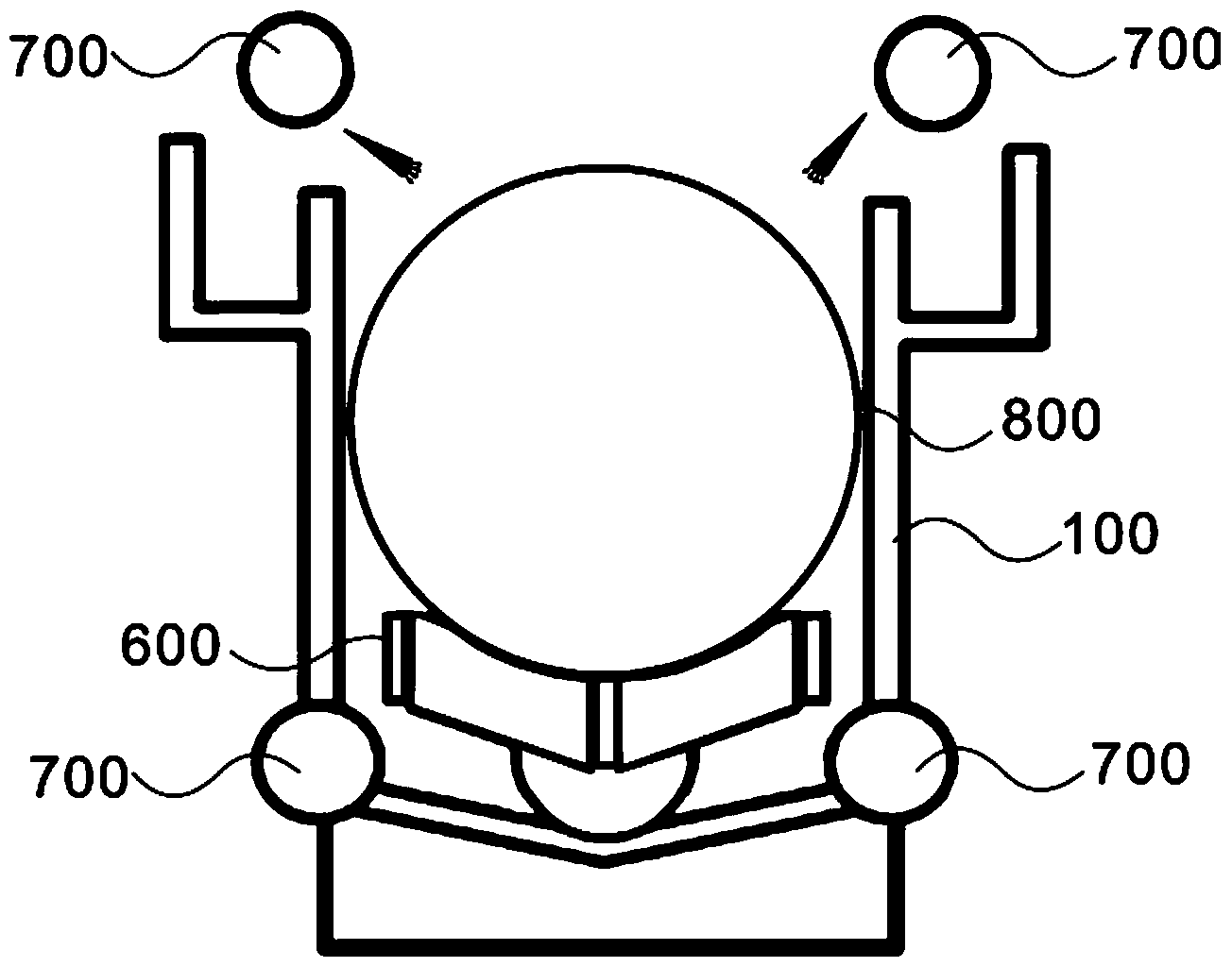
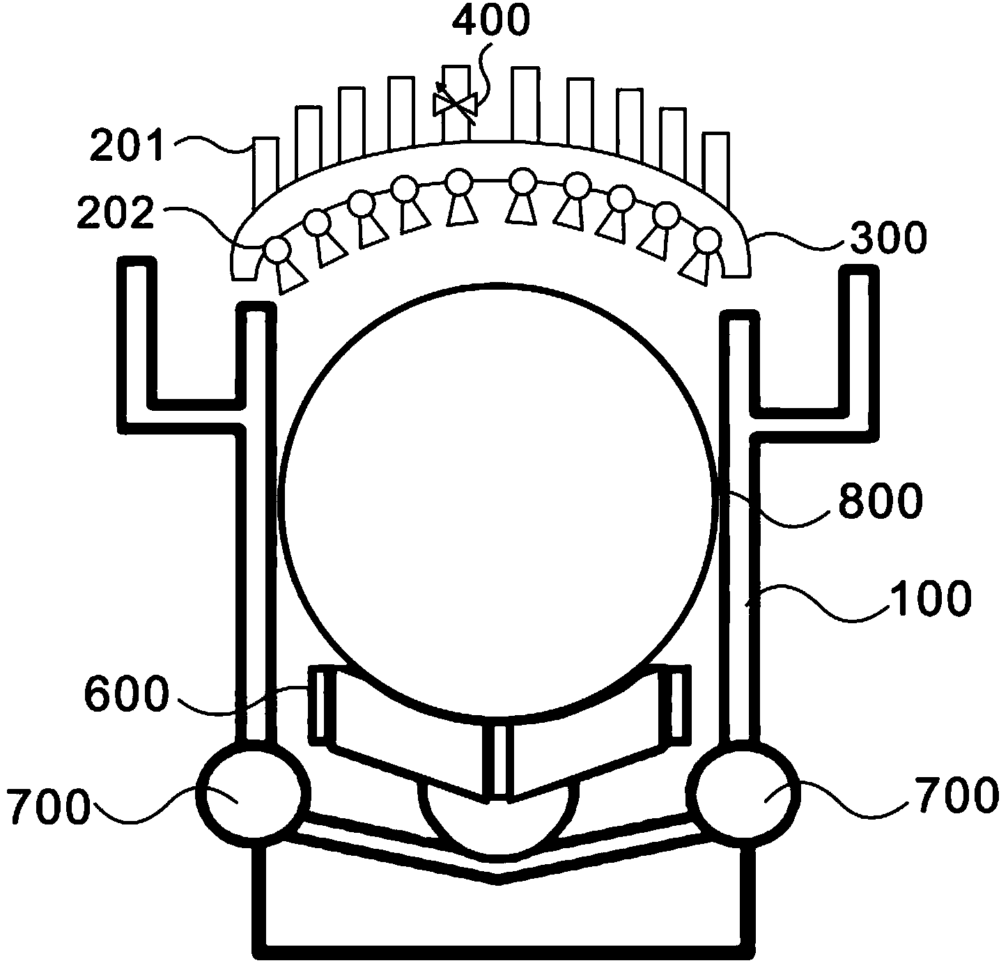
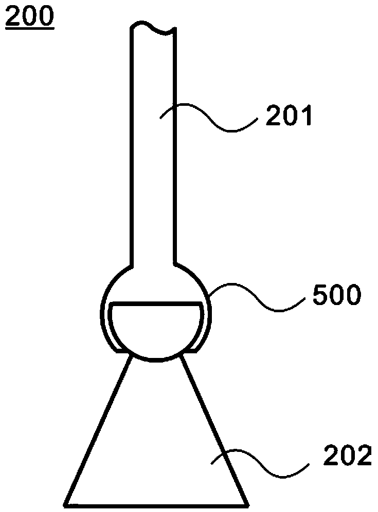
[0023] Such as figure 2 as shown, figure 2 It is a structural schematic diagram of a cleaning tank for cleaning semiconductor wafers in the present invention. The present invention provides a cleaning tank for cleaning semiconductor wafers, including a cleaning tank body 100, a spray device 200, and a top of the cleaning tank body 100. There is a tank cover 300 for closing the cleaning tank body 100, and the tank cover 300 is provided with a spray device 200 for cleaning wafers; the spray device 200 includes several spray pipes 201 and several nozzles 202 connected thereto, the nozzles 202 are evenly distributed in a matrix on the tank cover 300 an...


PUM


Abstract

The invention provides a rinse tank for rinsing a semiconductor wafer and belongs to the technical field of the semiconductor wafer technology. The rinse tank comprises a rinse tank body and a sprinkler, wherein a tank cover used for sealing the rinsing tank body is arranged over the rinsing tank body, the sprinkler used for rinsing the wafer is arranged on the tank cover and comprises multiple sprinkler pipes and multiple nozzles communicated with the sprinkler pipes, the nozzles are evenly distributed on the tank cover in a matrix mode, the sprinkling angles of the nozzles can be adjusted, and valves used for controlling rinsing fluid to pass through are arranged on the sprinkler pipes. According to the rinse tank, the tank cover is arranged on the upper portion of the rinse tank, the multiple nozzles with adjustable sprinkling angles are evenly distributed on the tank cover, the rinsing fluid can be jetted to rinse the wafer from different directions, and different positions and angles of the wafer can be covered; the rinsing capacity is higher, the rinsing surface is wider, rinsing time can be shortened, and the yield can be increased.

Description

technical field [0001] The invention belongs to the technical field of semiconductor wafer technology, in particular to a cleaning tank for cleaning semiconductor wafers. Background technique [0002] As the feature size of integrated circuits enters the deep submicron stage, the cleanliness of the wafer surface required in the integrated circuit wafer manufacturing process is becoming more and more stringent. In order to ensure the cleanliness of the surface of the wafer material, the manufacturing process of the integrated circuit There are hundreds of cleaning processes in the production line, and the cleaning process accounts for 20% of the entire manufacturing process. [0003] Traditionally, tank-type cleaning equipment with relatively high output is used to clean the surface of the wafer. The main cleaning steps of the cleaning equipment are generally cleaning and soaking in chemical liquid, and then cleaning with water. After the wafer is cleaned and soaked in chemi...

Claims


Application Information

Patent Timeline
Patent Type & Authority Applications(China)
IPC IPC(8): H01L21/67
CPCH01L21/67023
Inventor 李芳陈锟朱也方
Owner SHANGHAI HUALI MICROELECTRONICS CORP
Why Eureka
Try Eureka