Organic light emitting diode display pane

A technology for light-emitting diodes and display panels, which is applied to electrical components, electrical solid-state devices, circuits, etc., can solve the problems of narrow auxiliary electrode trace width and large trace resistance, and achieves favorable voltage drop, increased contact area, The effect of reducing trace resistance

Active Publication Date: 2014-06-18
HISENSE VISUAL TECH CO LTD
View PDF5 Cites 3 Cited by
  • Summary
  • Abstract
  • Description
  • Claims
  • Application Information

AI Technical Summary

Problems solved by technology

[0007] The invention provides an organic light emitting diode display panel to solve the problems of narrow auxiliary electrode wiring width and large wiring resistance in the prior art

Method used


Image

  • Organic light emitting diode display pane
  • Organic light emitting diode display pane
  • Organic light emitting diode display pane

Examples


Embodiment 1

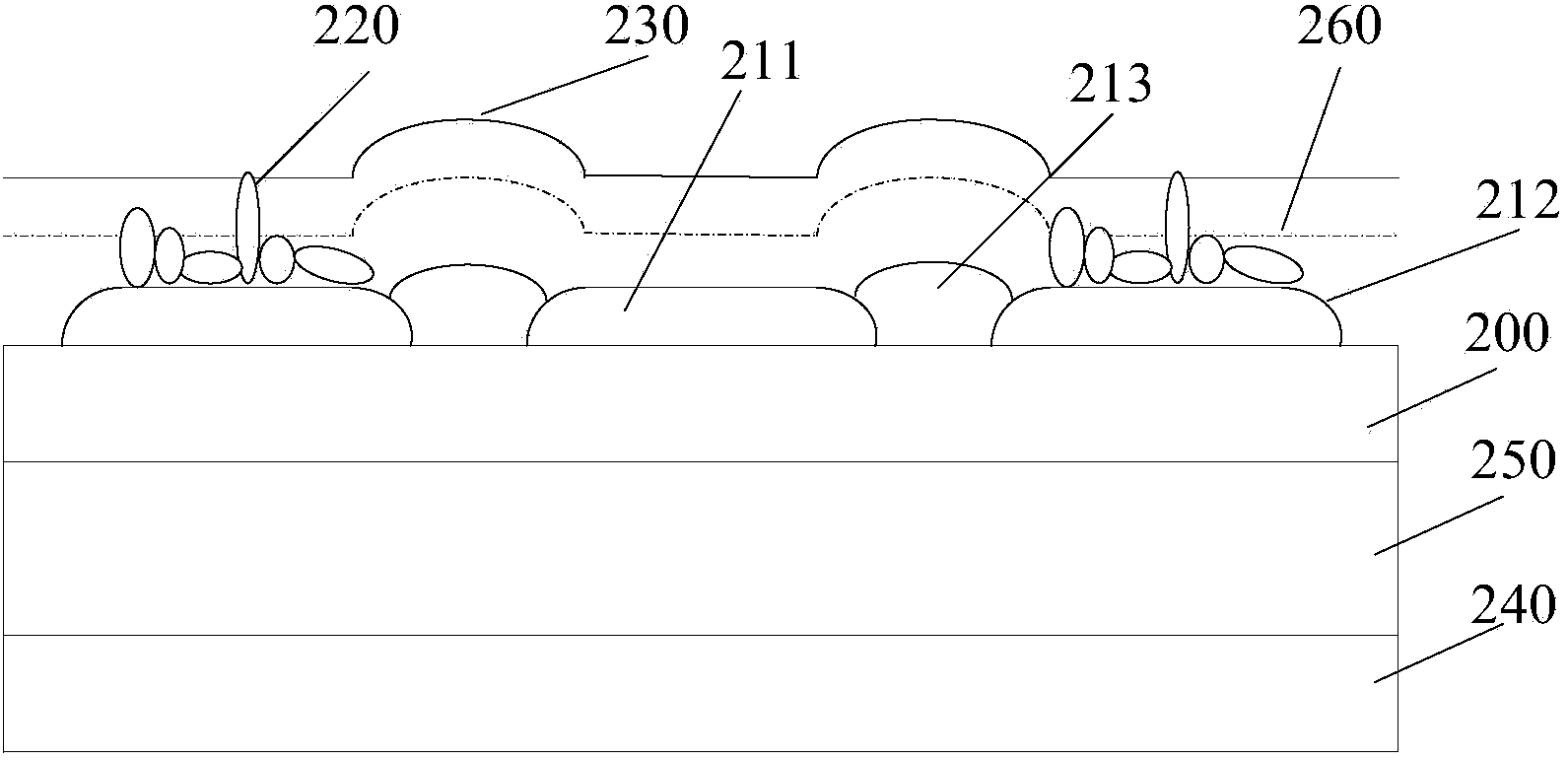
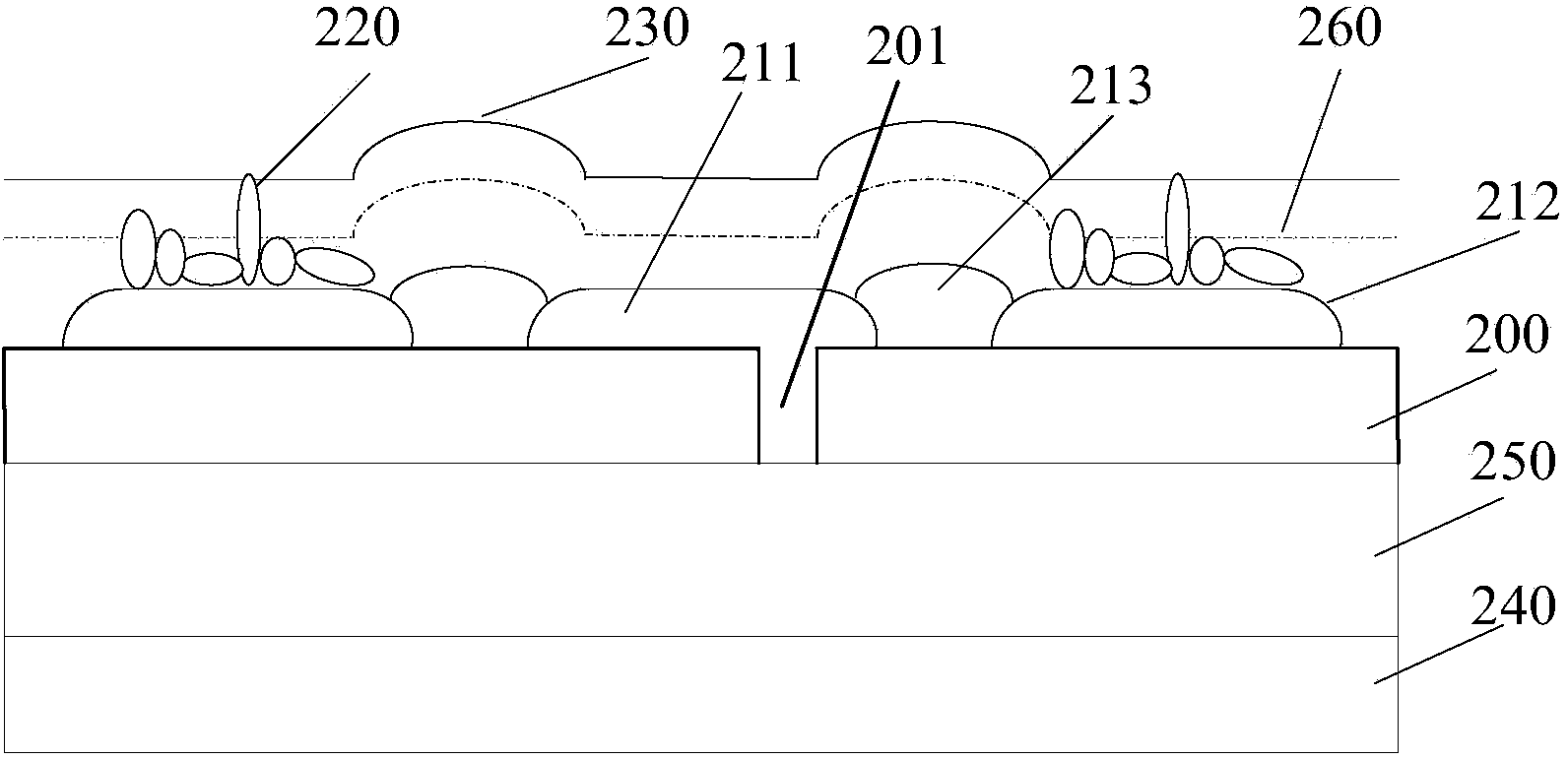
[0025] refer to figure 2 , which shows the structure diagram of the OLED display panel provided by Embodiment 1 of the present invention.

[0026] This embodiment provides a top-emitting AMOLED display panel, including: a planarization layer 200, an opaque electrode 211, an auxiliary electrode 212, a pixel definition layer 213, a conductive functional layer 220, a transparent electrode 230, a base substrate 240, and an organic functional layer 250 and an insulating organic layer 260 .

[0027] Wherein, the substrate 240 is basically located at the bottom of the OLED display panel, and an organic functional layer 250 is arranged on it, and the organic functional layer 250 is covered with a planarization layer 200; an opaque electrode 211 and an auxiliary electrode 212 are arranged on the planarization layer 200; The opaque electrode 211 and the auxiliary electrode 212 are covered with an insulating organic layer 260 ; the insulating organic layer 260 is covered with a transpa...


PUM


Abstract

The invention provides an organic light emitting diode display panel, which aims at solving the problems of narrower routing width and larger routing resistance of an auxiliary electrode of the prior art. The display panel comprises a substrate 240, an organic function layer 250 and a flattening layer 200, wherein an opaque electrode 211, the auxiliary electrode 212, an insulation organic layer 260 and a transparent electrode layer 230 are arranged on the flattening layer 200, the insulation organic layer 260 is covered on the opaque electrode 211 and the auxiliary electrode 212, the transparent electrode layer 230 is arranged on the insulation organic layer 260, a pixel defining layer 213 is positioned between the opaque electrode 211 and the auxiliary electrode 212, and is in contact with the two adjacent ends of the opaque electrode 211 and the auxiliary electrode 212, a conductive function layer 220 is arranged on the opaque electrode 211, the thickness of the conductive function layer 220 is greater than the thickness of the insulation organic layer 260, and the auxiliary electrode 212 is connected with the transparent electrode layer 230 through the conductive function layer 220.

Description

technical field [0001] The invention relates to the technical field of displays, in particular to an organic light emitting diode display panel. Background technique [0002] OLED (Organic Light-Emitting Diode, Organic Light-Emitting Diode) displays are technically divided into passive PMOLED (Passive matrix OLED) and active AMOLED (Active matrix OLED). Taking AMOLED as an example, its core technology includes Thin Film Transistor (TFT) devices and pixel drive circuits, OLED full-color technology and packaging. It can also be divided into bottom-emitting AMOLED and top-emitting AMOLED, as well as double-sided emission. [0003] Among them, the OLED device of top-emitting AMOLED is between the transparent electrode and the opaque electrode. The opaque electrode is fabricated together with the pixel driving circuit, while the transparent electrode is located on the other side of the OLED device. The transparent electrode is made of a metal material with a thickness less than ...

Claims


Application Information

Patent Timeline
IPC IPC(8): H01L27/32
Inventor 路林曹建伟刘卫东
Owner HISENSE VISUAL TECH CO LTD
Why Eureka
Try Eureka