Printed circuit board

A technology of printed circuit boards and conductive layers, applied in the direction of printed circuit components, etc., can solve the problems of small trace width and increase PCB manufacturing cost, and achieve the effect of improving power supply and return flow capacity, enhancing stability, and facilitating heat conduction

Inactive Publication Date: 2014-12-10
COMBA TELECOM SYST CHINA LTD
View PDF6 Cites 0 Cited by
  • Summary
  • Abstract
  • Description
  • Claims
  • Application Information

AI Technical Summary

Problems solved by technology

For packaged devices with a pad spacing of less than 0.8 mm, the trace width between the two isolation pads is smaller. To meet the current low-voltage and high-current requirements, it can be solved by increasing the number of power plane layers, but this will Increase the manufacturing cost of PCB

Method used


Image

  • Printed circuit board
  • Printed circuit board
  • Printed circuit board

Examples


Embodiment Construction

[0016] According to the resistance formula: R = ρ l A

[0017] Among them, ρ is the resistivity, l is the length of the wire, A is the cross-sectional area,

[0018] In the case of constant resistivity and thickness, the trace area should be increased as much as possible.

[0019] In addition, according to the ideal return path ground bounce voltage drop formula:

[0020] Among them, V gb is the ground bounce voltage, L total is the total return path inductance, L b is the local self-inductance, L ab is the local mutual inductance,

[0021] It can be deduced that when the signal edge change rate cannot be reduced and the number of layers of the PCB return path cannot be reduced, the trace width should be increased as much as possible.

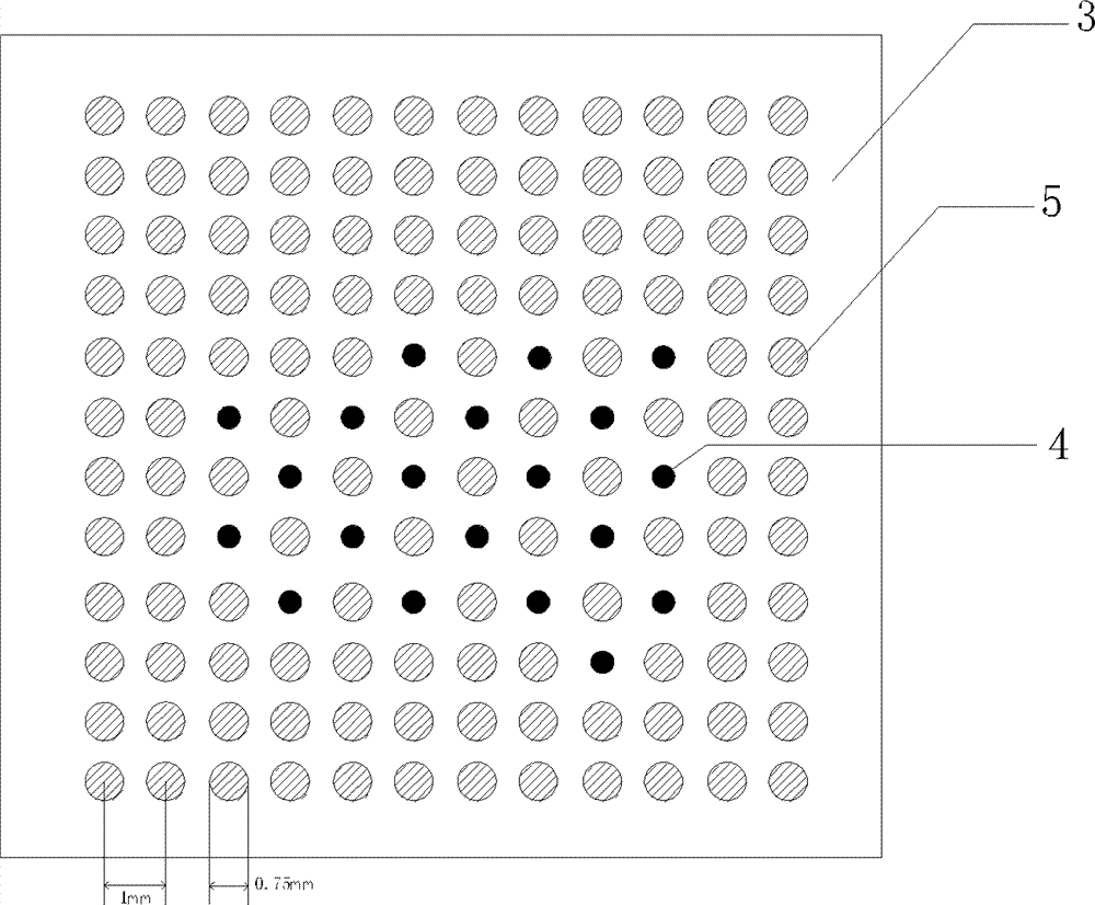
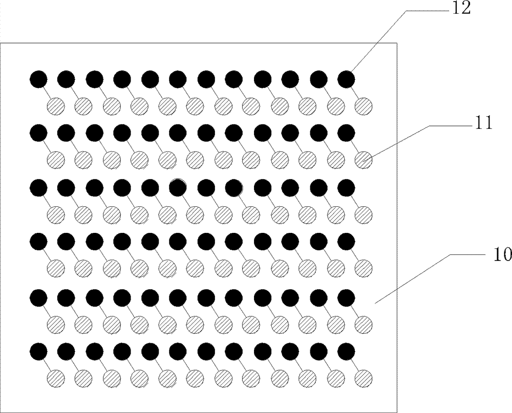
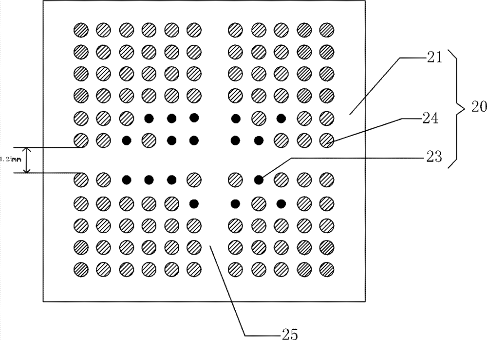
[0022] The PCB board of the present invention includes a surface layer board 10 , a power plane layer board 20 , a ground layer board 30 and a bottom layer boar...


PUM


Abstract

The invention discloses a printed circuit board (PCB), which comprises a surface layer board, a power plane layer board and a grounding layer board, which are stacked, wherein the surface of the power plane layer board is an electroconductive layer and is provided with power connecting holes and isolation bonding pads. A cross main channel is arranged on the electroconductive layer, and the power connecting holes and the isolation bonding pads are arranged in four quadrant areas formed by the main channel. Compared with the prior art, the PCB provided by the invention has the advantages that the line routing width on a power plane and a ground plane is increased, the power supply and backflow capacities of power supply and ground systems in an BGA (Ball Grid Array) area are improved obviously, meanwhile, the routing and fan-out areas of other signal lines are not influenced and occupied, the number of PCB application numbers can be decreased, the number of filter capacitors capable of being placed in a bottom-layer core power supply area right below a chip is increased, and thus, the filter effect of the power supply and the stability of the power supply system are enhanced and heat conduction is facilitated.

Description

technical field [0001] The present invention relates to a printed circuit board (PCB). Background technique [0002] With the development trend of miniaturization and functional integration of electronic products, higher and higher requirements are put forward for PCB boards using ball grid array structure (BGA: Ball Grid Array) packaging technology. For example, the number of layers of the PCB board needs to reach 4-6 layers or more, and the distribution of the BGA pads of the PCB board also needs to be very dense, and the distance between adjacent BGA pads is also getting smaller and smaller, such as , 1 mm pad pitch, 0.8 mm pad pitch, 0.5 mm pad pitch, etc. In the PCB board design process, it is also necessary to lay out via holes. A layer of copper foil is plated on the inner wall of the via holes for interconnection between different signal layers and plane layers, and to connect the same signals of different signal layers together. [0003] At the same time, with the...

Claims


Application Information

Patent Timeline
Patent Type & Authority Patents(China)
IPC IPC(8): H05K1/02
Inventor 张露露
Owner COMBA TELECOM SYST CHINA LTD
Why Eureka
Try Eureka