Semiconductor structure and forming method thereof

A semiconductor and sacrificial layer technology, applied in the field of semiconductor structure and its formation, can solve the problems of difficulty in controlling line width and line spacing at the same time, affecting the roughness of the edge of the scribe line, and insufficient merging of side walls, etc., so as to reduce the impact and reduce the The effect of using the number of layers to improve product yield

Pending Publication Date: 2021-12-07
SEMICON MFG INT (SHANGHAI) CORP +1
View PDF0 Cites 0 Cited by
  • Summary
  • Abstract
  • Description
  • Claims
  • Application Information

AI Technical Summary

Problems solved by technology

But for some special designs, such as static random access memory (SRAM, Static Random-Access Memory), it is necessary to introduce non-uniform fin pitch to obtain process window
[0003] At present, non-uniform fin spacing can be obtained by sidewall merging, but there are many process problems in this method, for example, the number of required mask layers is large, the process is complicated, and it is prone to insufficient sidewall merging Phenomenon, the removal of the mask layer will affect the line edge roughness (LER, Line Edge Roughness), and it is difficult to control the line width and line spacing at the same time

Method used


Image

  • Semiconductor structure and forming method thereof
  • Semiconductor structure and forming method thereof
  • Semiconductor structure and forming method thereof

Examples


Embodiment Construction

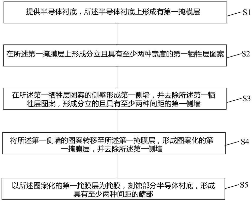
[0024] The following description provides specific application scenarios and requirements of the application, with the purpose of enabling those skilled in the art to manufacture and use the contents of the application. Various local modifications to the disclosed embodiments will be readily apparent to those skilled in the art, and the general principles defined herein may be applied to other embodiments and embodiments without departing from the spirit and scope of the application. application. Thus, the application is not limited to the embodiments shown, but is to be accorded the widest scope consistent with the claims.

[0025] The technical solution of the present invention will be described in detail below in conjunction with the embodiments and the accompanying drawings.

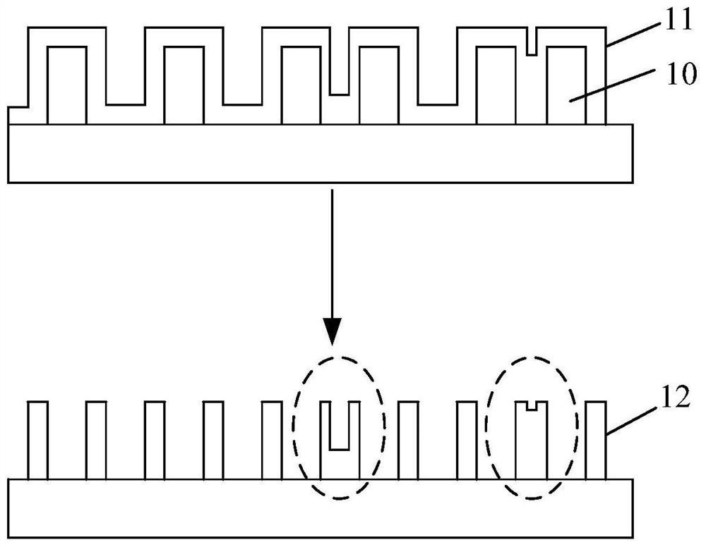
[0026] Such as figure 1 As shown, some semiconductor devices need a special design to meet the requirements of process manufacturing, such as SRAM needs to introduce non-uniform fin spacing to obta...


PUM

PropertyMeasurementUnit
thicknessaaaaaaaaaa
sizeaaaaaaaaaa
thicknessaaaaaaaaaa

Abstract

The invention provides a semiconductor structure and a forming method thereof, and the method comprises the steps: providing a semiconductor substrate, and forming a first mask layer on the semiconductor substrate; forming discrete first sacrificial layer patterns with at least two widths on the first mask layer; forming first side walls on the side walls of the first sacrificial layer patterns, and removing the first sacrificial layer patterns to form discrete first side walls with at least two intervals; transferring the pattern of the first side wall to the first mask layer to form a patterned first mask layer, and removing the first side wall; and etching a part of the semiconductor substrate by taking the patterned first mask layer as a mask to form fin parts with at least two intervals. According to the formation method of the invention, non-uniformly distributed fins can be obtained.

Description

technical field [0001] The present application relates to the field of semiconductor technology, in particular to a semiconductor structure and a method for forming the same. Background technique [0002] As the size of the fin semiconductor structure shrinks to 14nm or below, it is shortened by the self-aligned double patterning (SADP, Self-Aligned Double Patterning) process or the self-aligned quadruple patterning (SAQP, Self-Aligned Quadruple Pattern) process. Fin pitch (Fin pitch) to increase device density. However, for some special designs, such as Static Random-Access Memory (SRAM, Static Random-Access Memory), non-uniform fin spacing needs to be introduced to obtain a process window. [0003] At present, non-uniform fin spacing can be obtained by sidewall merging, but there are many process problems in this method, for example, the number of required mask layers is large, the process is complicated, and it is prone to insufficient sidewall merging Phenomenon, the r...

Claims


Application Information

Patent Timeline
Patent Type & Authority Applications(China)
IPC IPC(8): H01L21/336H01L21/311H01L21/8238
CPCH01L29/6656H01L29/6653H01L21/823821H01L21/31116H01L21/31144
Inventor 张冬平
Owner SEMICON MFG INT (SHANGHAI) CORP
Why Eureka
Try Eureka